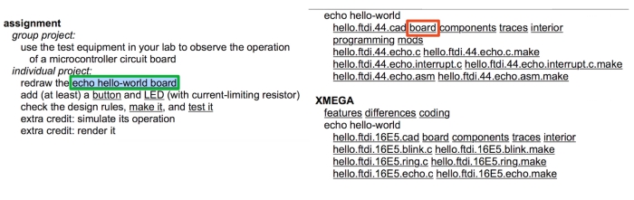
- Redraw the echo hello-world board (individual)
- Add (at least) a button and LED (with current-limiting resistor) (individual)
- Simulate its operation (Extra, individual)
- Render it (Extra, individual)
- Use the test equipment in your lab to observe the operation of a microcontroller
circuit board (group) (LINK)
Learning basics of embedded programming
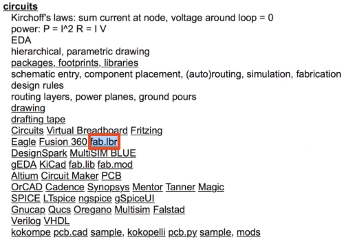
This week´s assigment was to redraw the hello-world board. I prepared by acquiring fab lib. and the hello-world board file from this week´s project site. This was done as seen bellow:First I opened this week´s lecture site and downloaded fab.lib:
Next I clicked "echo hello-world board" to transport to another page where I opened board layout link:
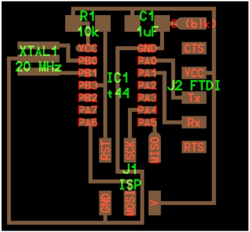
This layout picture showed all the parts I needed to build this week´s board:
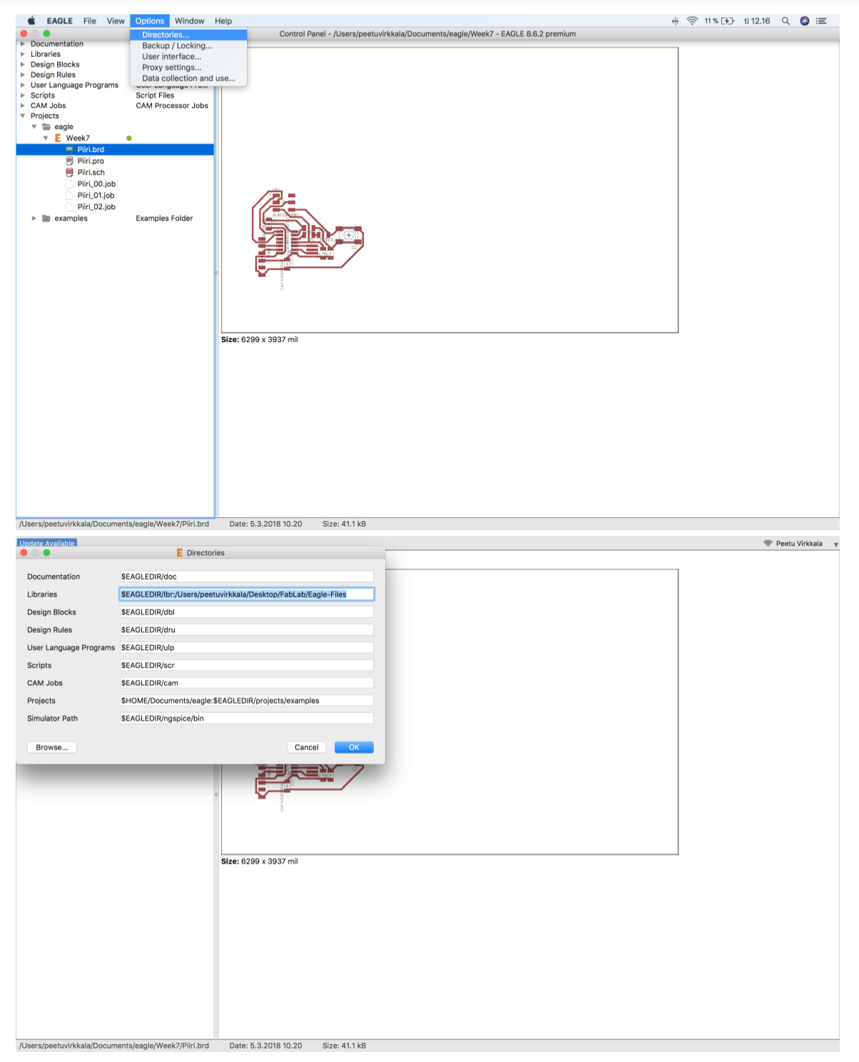
When this was done, I opened Eagle-software. To be able to use parts found in fablabs in Eagle, I added fab lib. to eagle as seen bellow. 1: Click Options < Directories, 2: Add fab lib. file address into "Libraries" slot and clicking OK button. Fab lib. is now added.
Then it was time create schematic for the board in Eagle. To do this, I used previously introduced hello-world board layout image as a reference and picked corresponding parts from fab lib. The process went forward as seen bellow:
First I created new schematic by clicking new > Schematic:
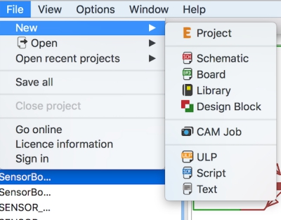
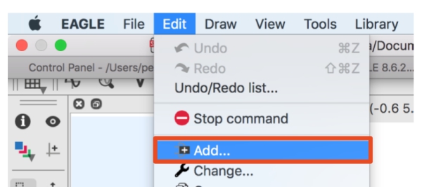
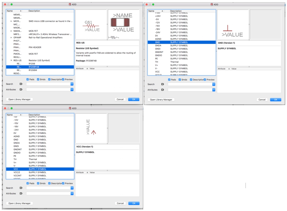
Next I clicked Edit > Add.. in Schematic to add fab lib. parts:
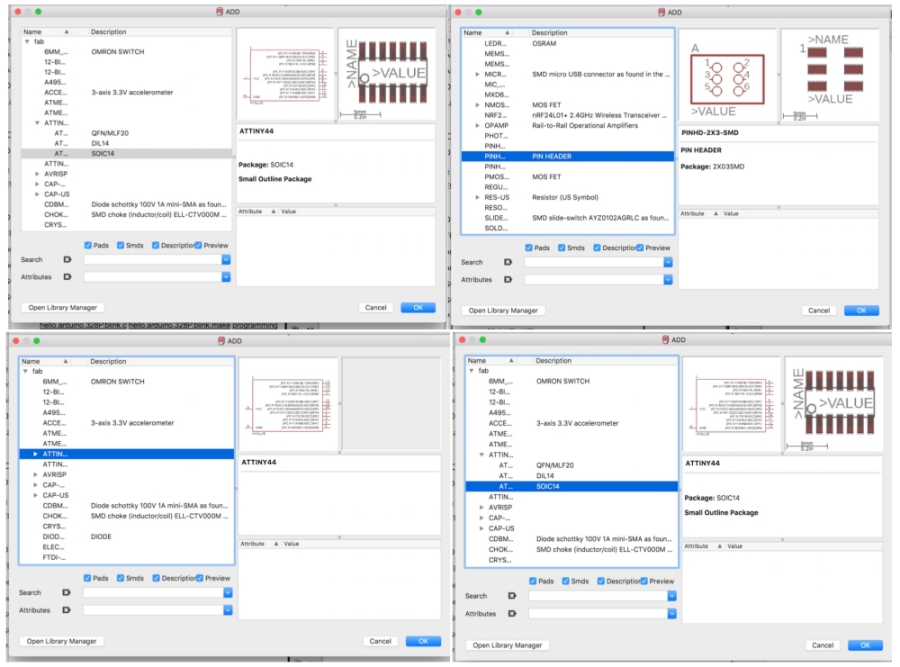
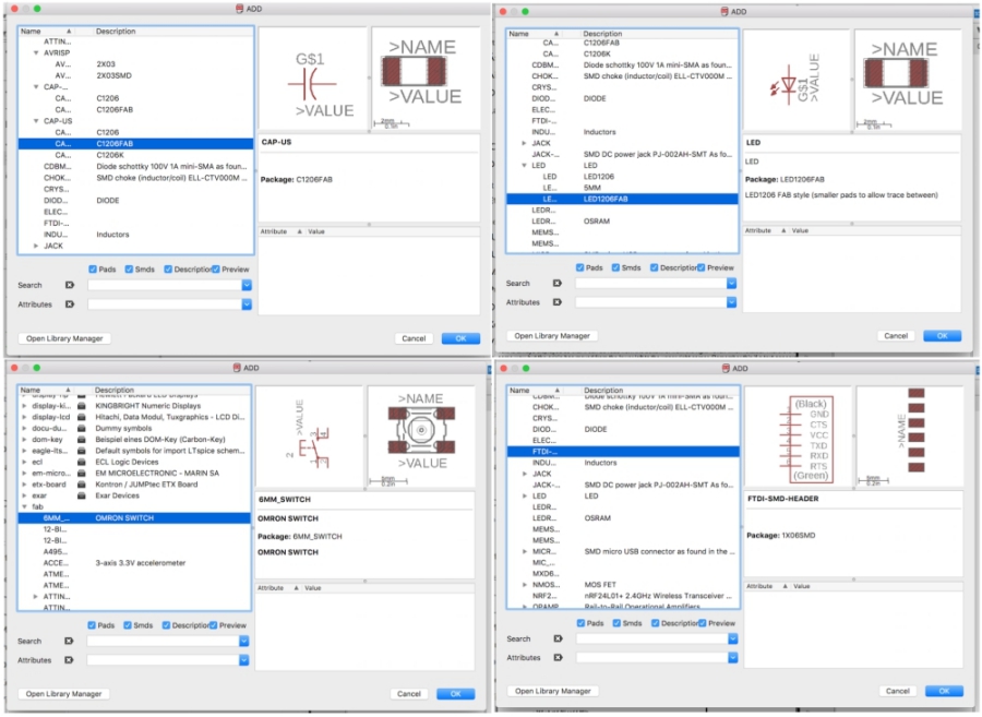
Then I found all the parts seen in the layout with the help of our instructor Antti. I added them one by one to my schematic:
After getting all the parts, the schematic looked like this:
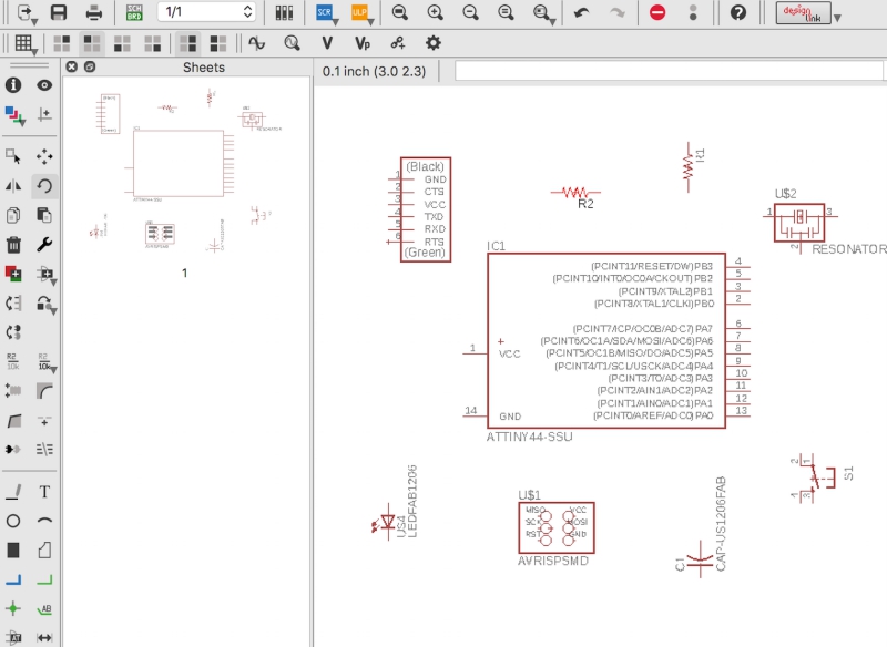
Next, I added electrical connections between the parts. as seen bellow:
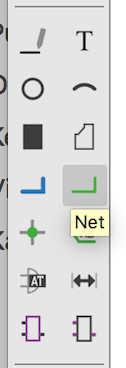
I began by chosing Net tool from toolbar on left:
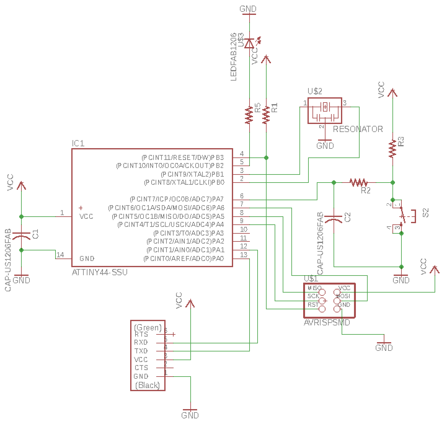
Then I drew connection between the boards as in the reference picture and used VCC and GND shortcut icons to connect VCC and GND connections. Final version of the board can be seen bellow:
Next, it was time to redrawn the board layout.
Redrawing the board layout
I began by moving to Eagle layout mode by clicking brb/sch icon on the top of the window: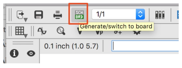
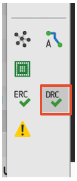
To use right settings, I opened "design rule check" window by clicking icon found from toolbar on left:
From there, I changed "16 mil" to few settings as can be seen bellow. This was done to easier designing and milling processes:
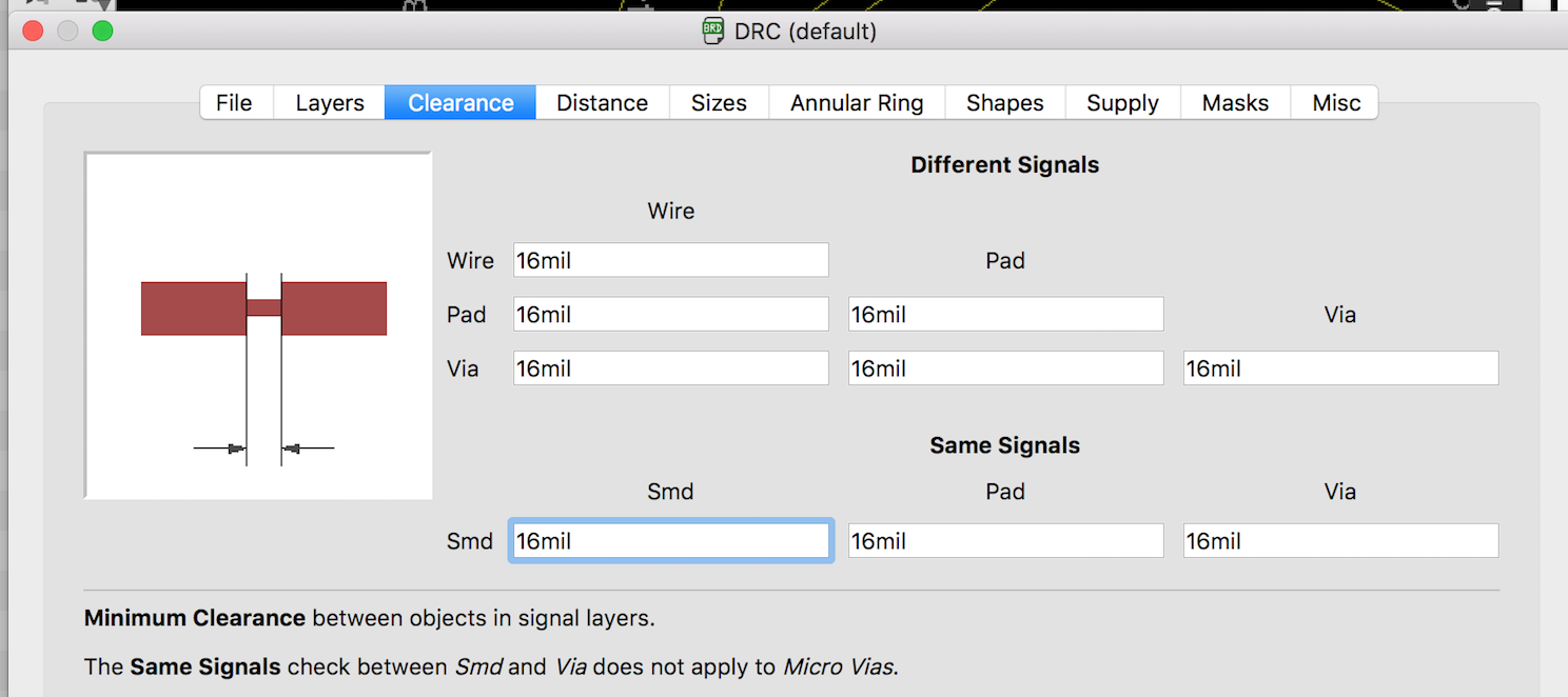
16 mil in Wire (PCB lines), Pad (point where component is soldered) and Via (point of transition in the PCB that transfers a trace between layers) columns and rows under the headline "Different Signals" ensures that there are at least 16 mil clearance between each of these parts when they come from different signals.
Under the headline "Same Signals" Wire, Pad and Via values ensure that there are at least 16 mil clearance between these parts when they come from same signals
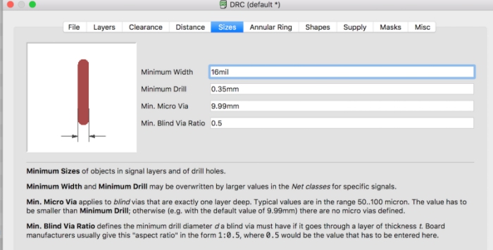
16 mil minimum width ensures that wire width is at least 16 mil all over the layout.
Then I put parts one by one on the black (board) area according to how I though the board would be layouted by dragging them with the mouse:
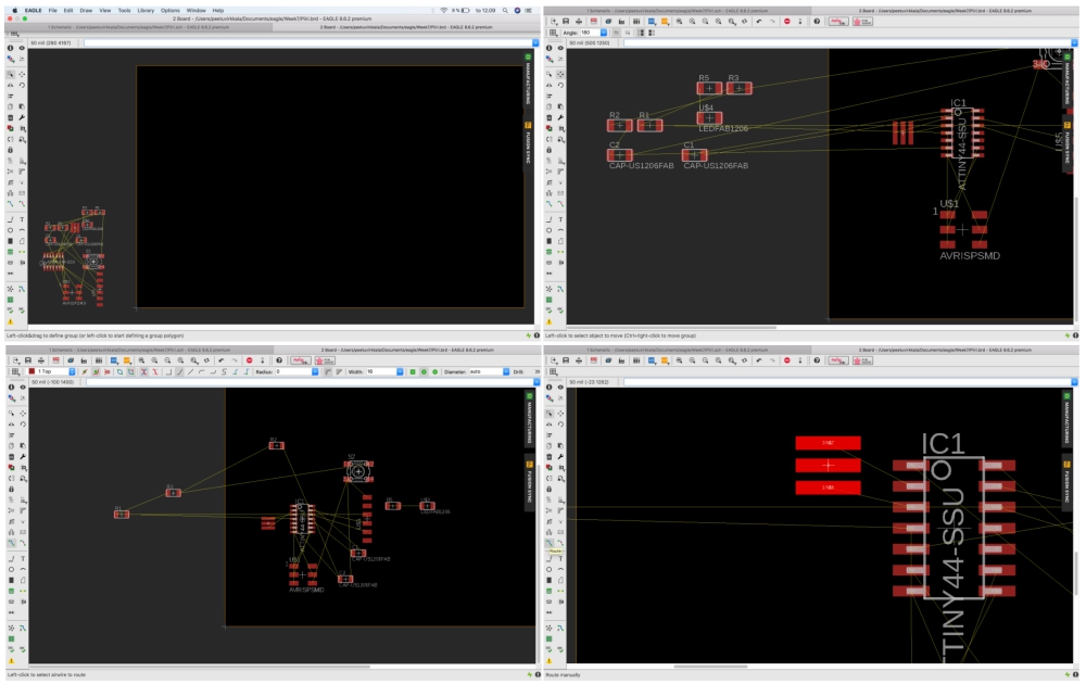
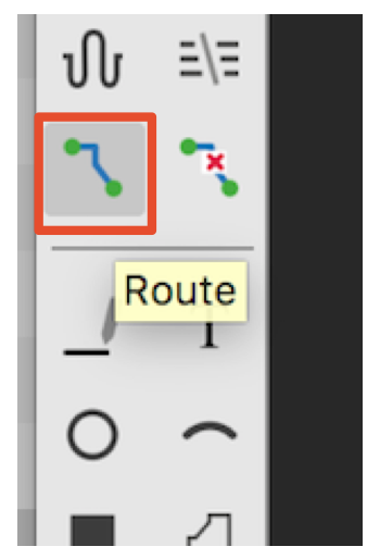
Next I used Route tool found from toolbar on left to draw routes between the components:
I followed Eagle´s yellow instruction lines to connect right parts together:
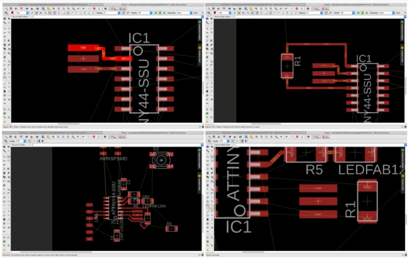
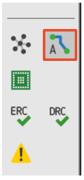
When I began to have problems in drawing the routes manually, I automatic router found from toolbar on left:
I used following settigns and clicked "continue"
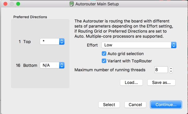
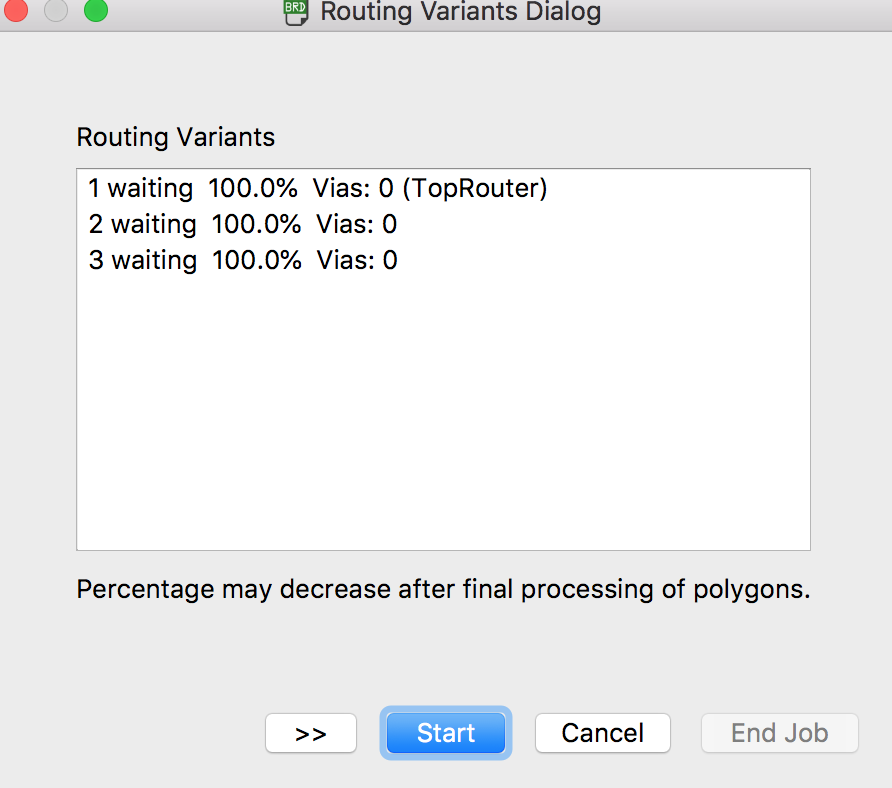
Then I clicked "start" and automatic route generating began. When it was ready, I choosed option with 100% and clicked "End job"
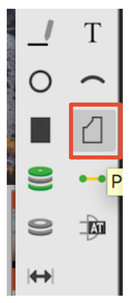
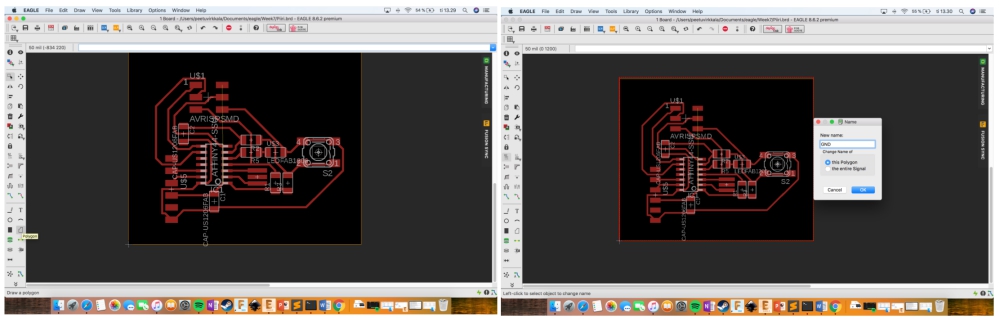
Parts were now connected properlly. Next I drew polygon around the circuit by using polygon tool foun from toolbar on left:
Then I named it as "GND" by writing the name on top of the screen and by pressing "Enter".
Then I clicked "Rattlenest" icon found form toolbar on left to create ground between the connected parts and the polygon:
Ground was now ready:
Next I prepared interior layout around the board. I chosed "polygon" tool from toolbar and chosed layer 46 "milling" and Width 40:

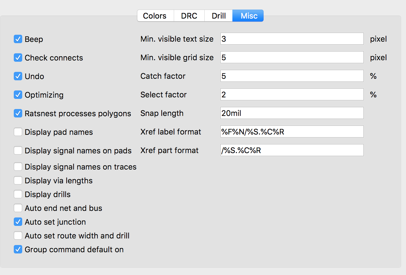
Then I drew polygon around the board and shrinked black area around the polygon. Then I opened Options > Set.. > Misc... and used following settings to hide part names from the layout:
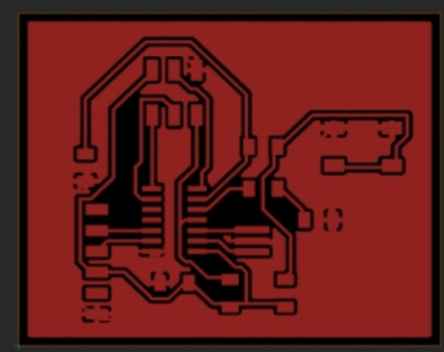
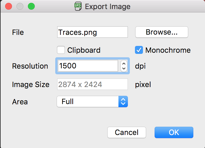
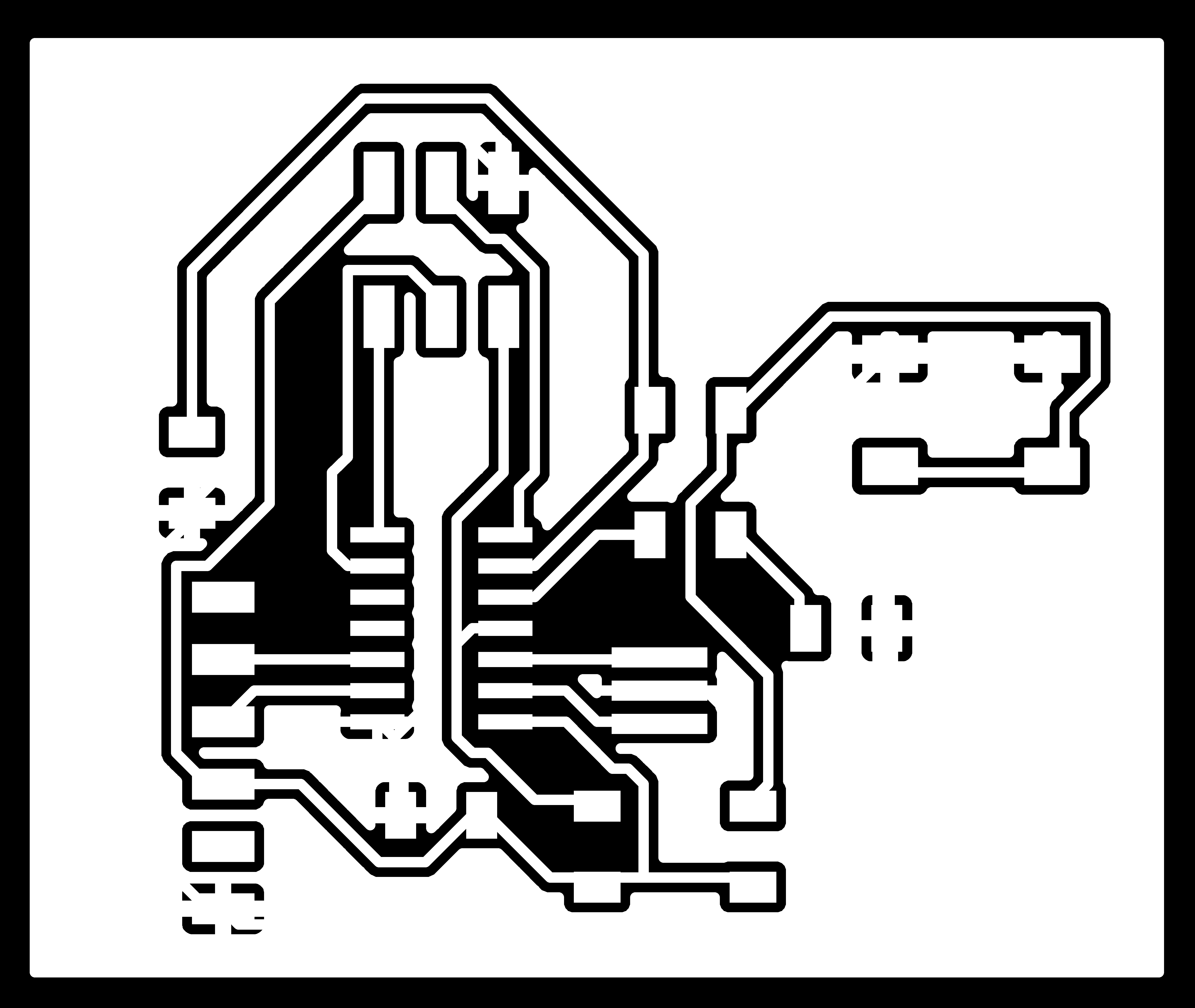
Then I chosed Layer 1 (traces) and saved it as a image by choosing File > Export > Image. I used following settings for exporting and saved the file as a PNG file:
Then I did same exporting process for Layer 46 (traces). The board layout was now ready.
Preparing and milling the board
Next I used fab modules like during the WEEK5 to create .rml traces and interior files for Rolland SRM milling machine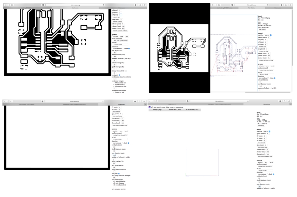
Cutting and assembling the board
I cut the board like during the WEEK5. End result was good as can be seen bellow: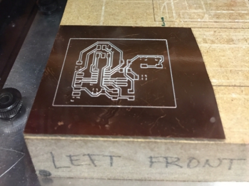
Then I soldered all the parts to the board as during the WEEK5 on their places. The end result before and after soldering the components can be seen bellow:
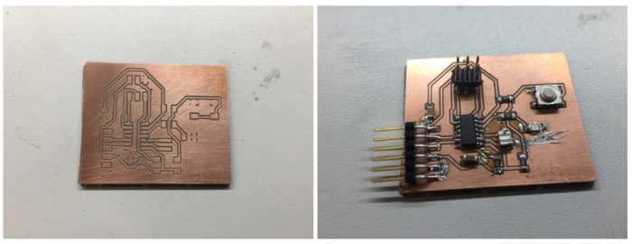
This week I didn´t have time to program the board so I will do it in future during the WEEK11.
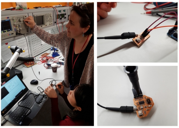
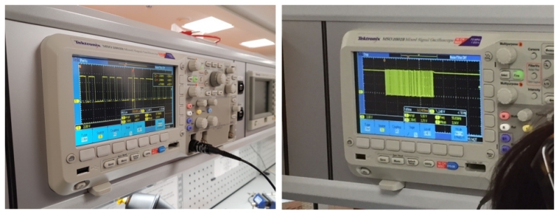
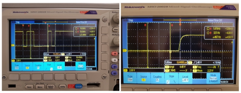
EXTRA: Group work - Observing microcontroller circuit board
Our group measured microcontroller circuit boards signals with oskiloscope
