Electronics design
Things to do:
2) Redraw the echo hello-world board, add (at least) a button and LED (with current-limiting resistor)
3) Check the design rules, make it, and test it
*Extra credit: simulate its operation / render it
Have I achieved this week's goals?
Basic approach needed
This week has been very demanding because of my lacks in electronics field. I've never studied it and I'm not familiar with its symbols, laws and so on. Anyway, I love learning new things and I decided to study a bit more on handbooks and I looked for some information on the Internet too. During my days of research, I took some notes (that will be useful in the near future). I carefully read this page, because it was a perfect introduction for my situation. It guided me throughout all the steps I needed to know. After having installed Eagle, I tried to understand how it works. I also studied some electronics basis here because I didn't know anything about them. After this theoretical part, I looked for the echo hello-board. I downloaded the .png file and I saved it on my computer. Then, I opened Eagle and I tried to import the library (fab.lbr) that contains all the essential components to redraw the PCB. I found some difficulties in adding the library on Eagle's projects folder! In fact, even if I added all the components in one time, when I opened Eagle, my library was not available and I had to add it each time I wanted to use it. How can I do? I'll find a solution!
Where's my library?
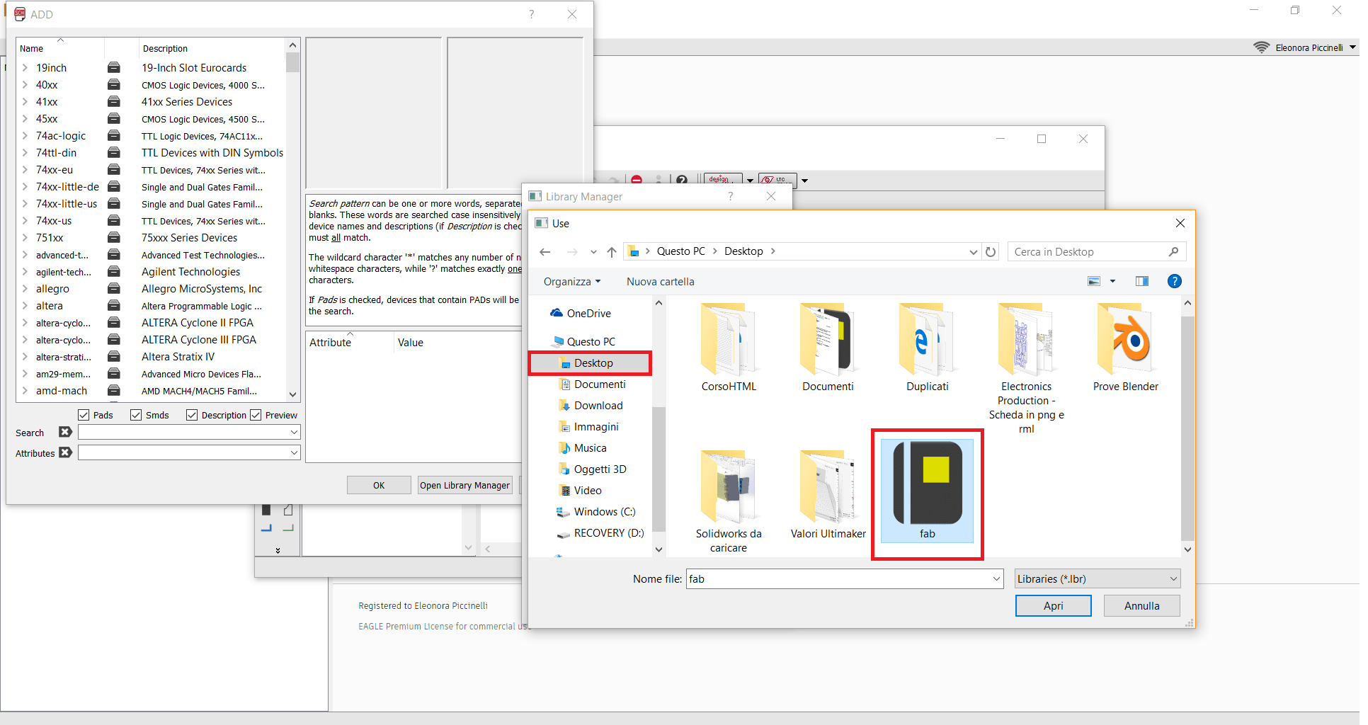
First, I tried to add the Fab Library clicking on the symbol that runs the command. In fact, I opened the Library Manager and I browse some folders looking for the download. After having opened it, I thought there was anything else to do. But I made a mistake.
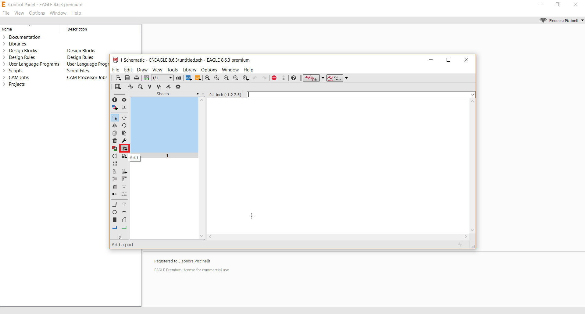
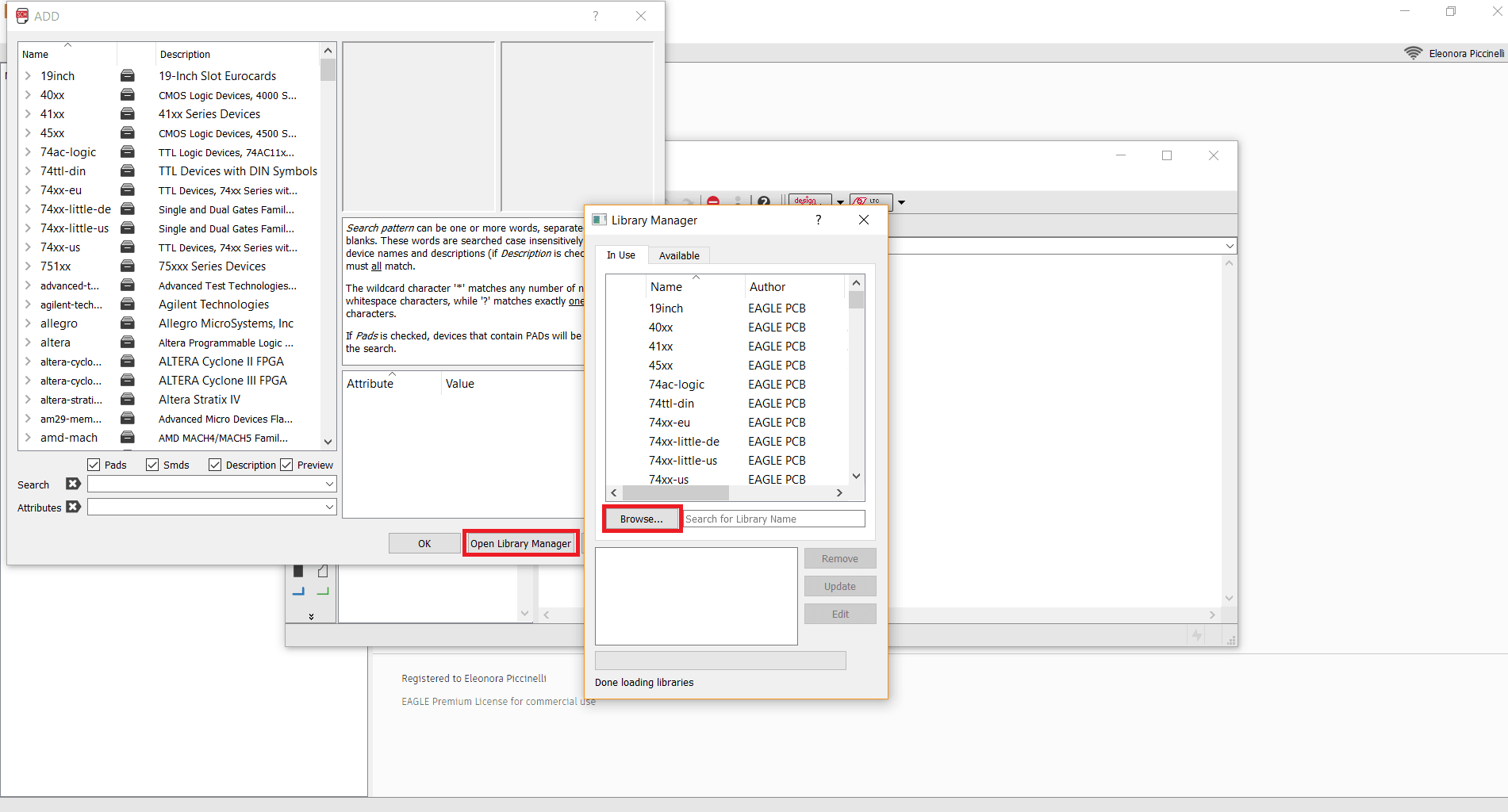
I discovered I forgot an essential step! I would have been opened the library folder on the left menu. There I found all the lists available and there was my library too. I understood it was necessary clicking on useand the grey button magically became green!! Now, when I open Eagle and I want to edit something on the schematic or start a new project, I don't have to upload my library again. In this way, is really practical and you have all your components always available and on the CAM software.
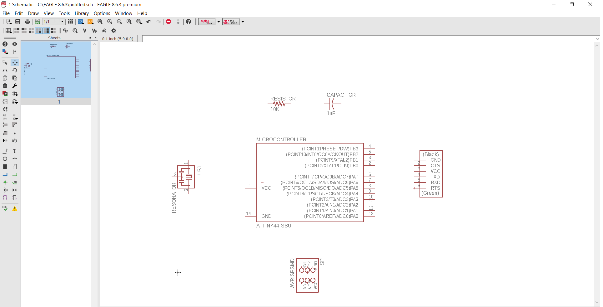
Redrawing the Hello-Board
Beginning my experience with the Eagle CAM, I understood a fundamental difference between the schematic sketch and the board (that contains all the physical components). If you want to see them, you can go on Digi-Key and you can see the shape they have and you can also buy them. I didn't think it was necessary following these steps. On the contrary, the program works as a 3D modeling software I used during the previous weeks. You first do a sketch and then, you have an other point of view to see your work (sketching the schematic to the board!). It exist a precise workflow. First of all, I decided to add all the components needed to create the Hello board. Considering the fact I don't know anything about electronics, I put the Neil's board image in front of me. This way helped me a lot, but I did a mistake anyway. In fact, I added a wrong components confusing it for the ATtiny 44. I thought all the schematics were quite similar, but I noticed I put a microcontroller with 4 sides pins, instead of the correct one (only 2 sides of pins). Fortunately, I found the error immediately and I deleted the wrong microcontroller and I put the correct one on my sketch. So, I began to positioning the components on eagle, trying to respect the position they have on the Neil's sample. Then I started linking all the components. I followed the basic procedure using the net command. Then, my instructors told me I would have been used the label command: the nets would have been invisibles and I would have been atributed a name on each side of each components. Sticking to reality, the sketch would have been nicer and easier to see eventually mistakes. I'll follow this kind of option the next time, avoiding the green labyrinth built by the nets scheme.
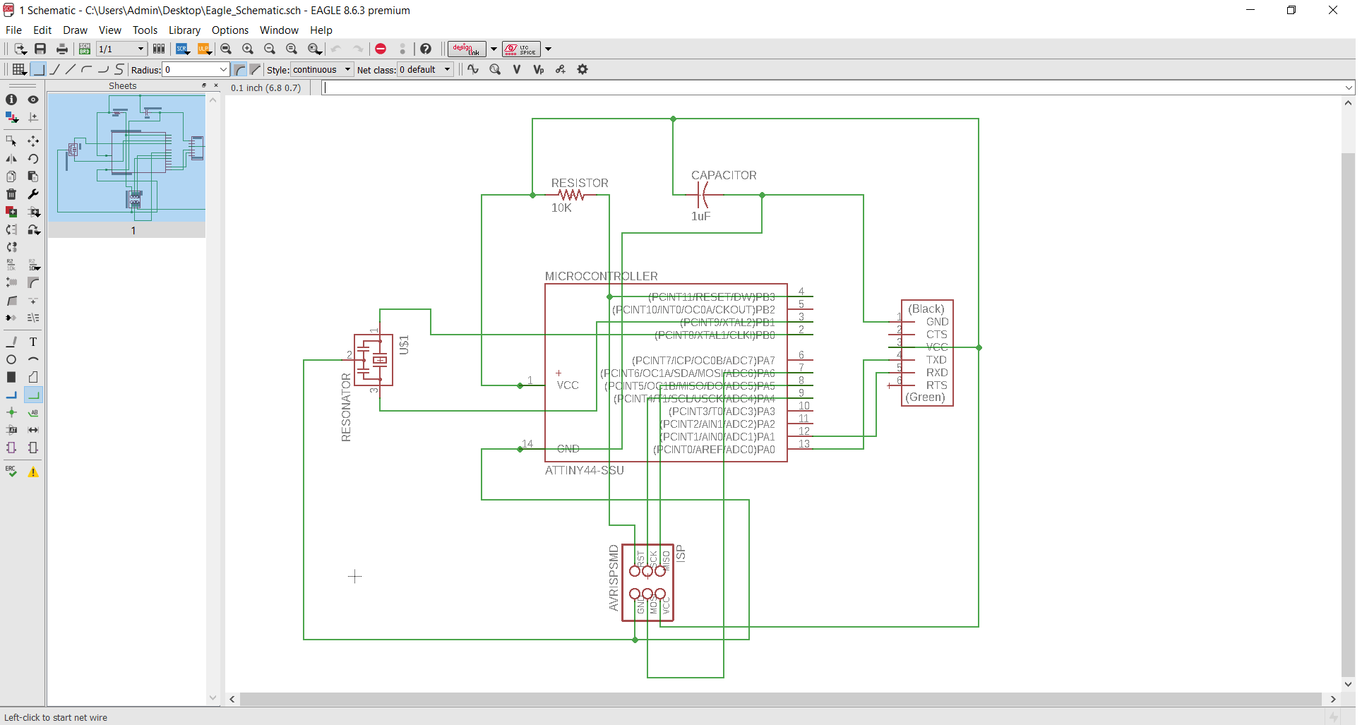
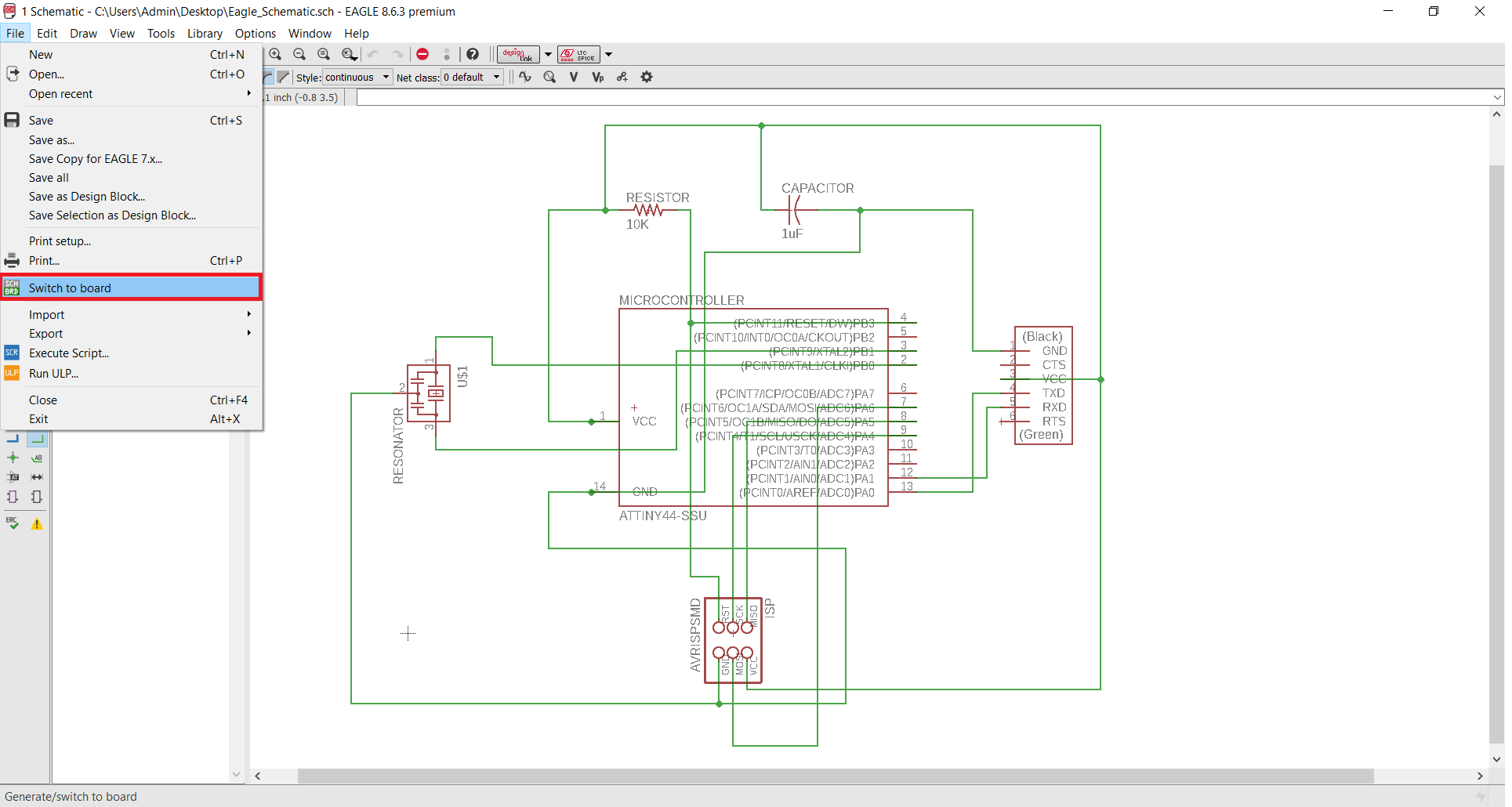
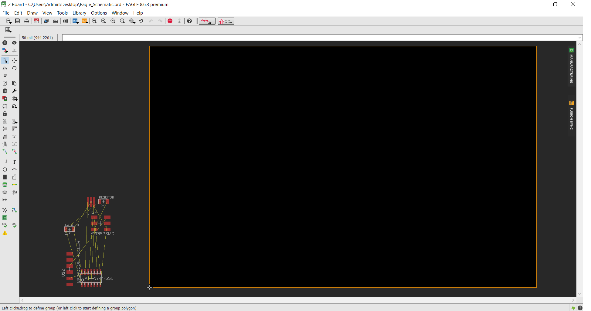
After some tests, components rotations and so on, I obtained the final version of my sketch. So, I decided to switch it on the board. At first sight, you have an other labyrinth of yellow lines and you have to move your components on the black area put on the right. After that, I unravel the lines, rotating the components and trying to move them closer to reduce the PCB dimensions.
Then, I went to Tools --> DRC and I set the options related to the wire clearance and size. In the screenshot below, you can see the values I used. After that, I wanted to draw the routes, but watching my area I noticed I didn't change the ISP position. So I had the ground in the internal part of the PCB. I simply rotated the components, putting the ground on the left side at the bottom. Finally I cliked on route command and I started drawing my traces.
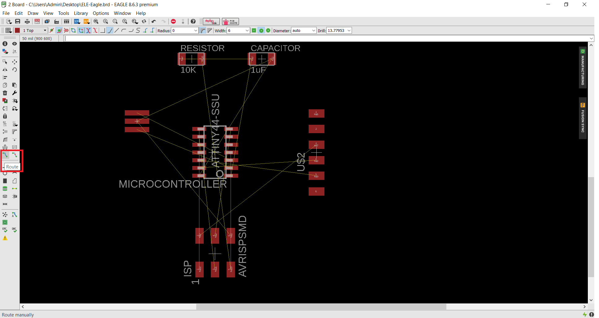
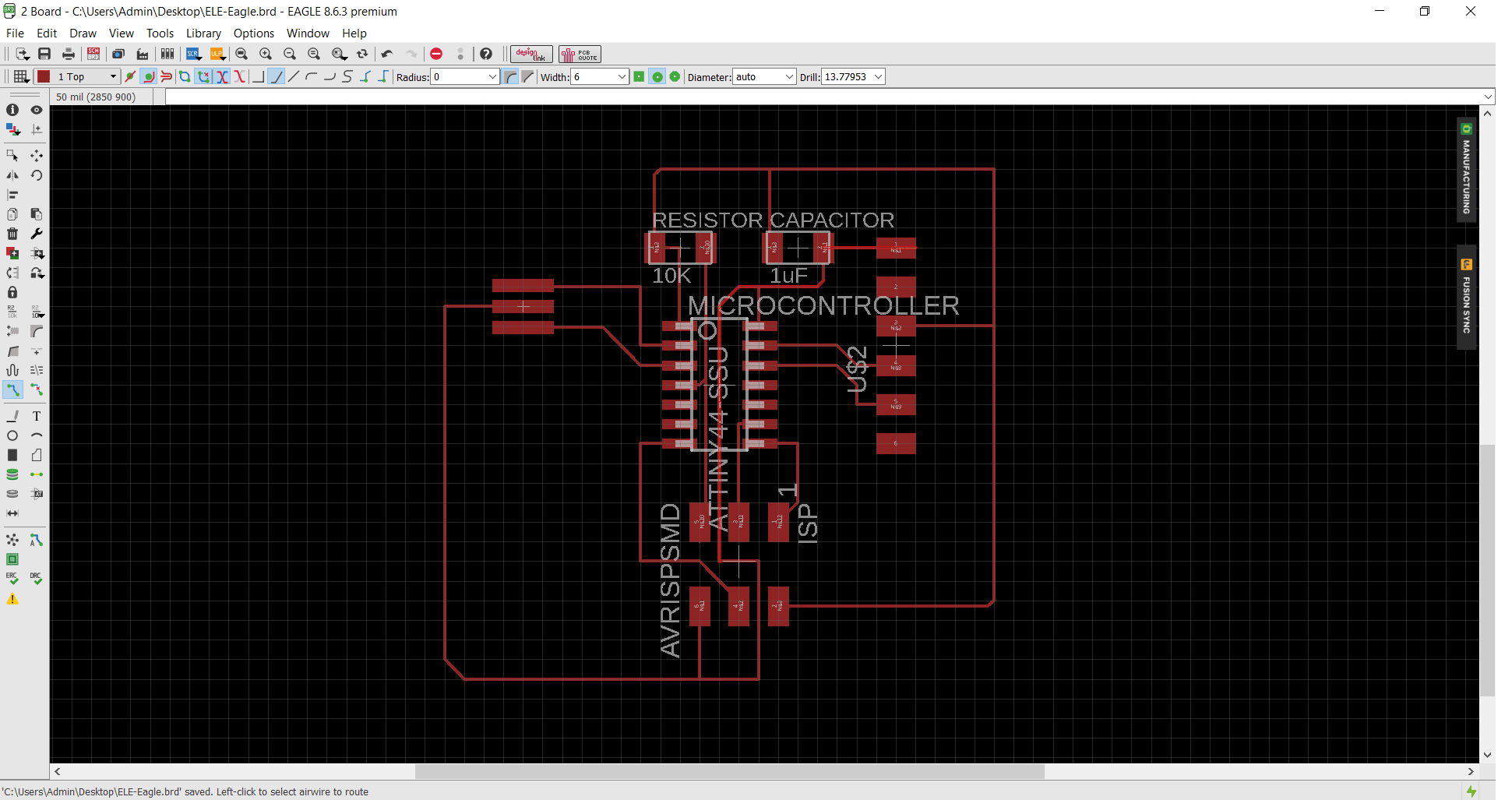
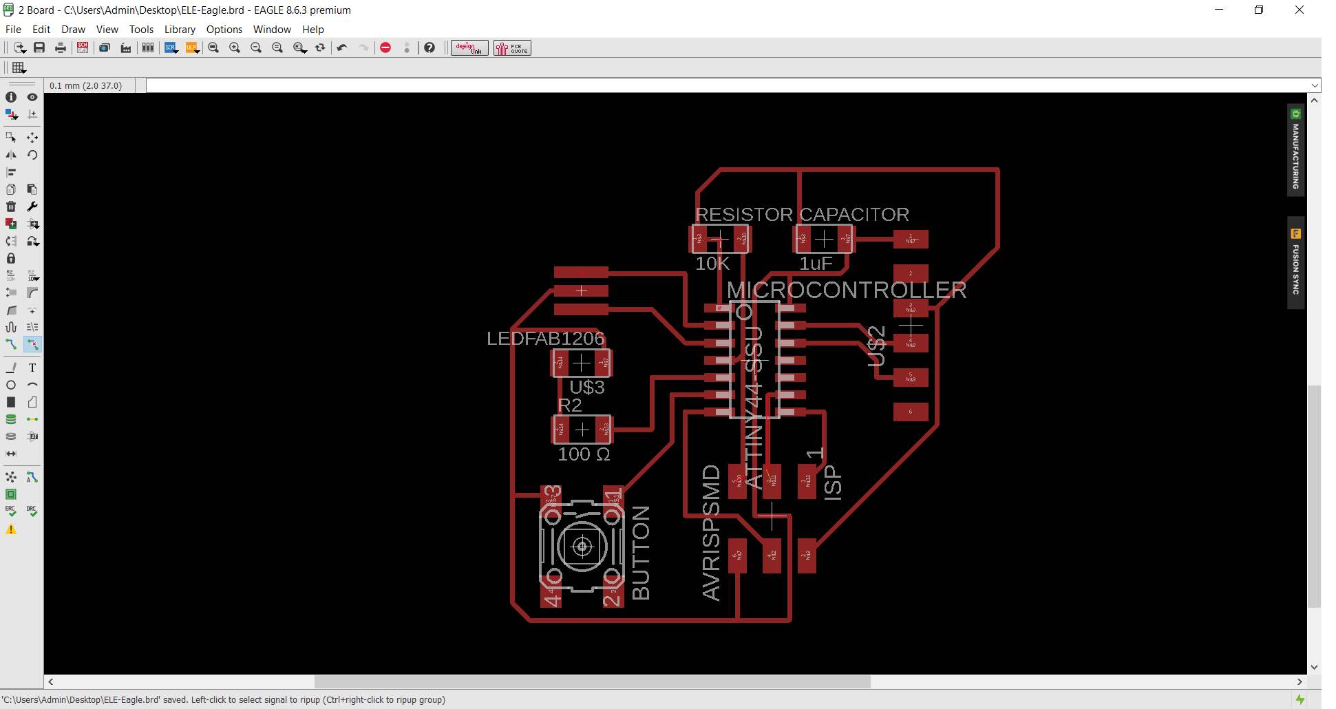
The thing I liked is referred to the yellow lines. They remains as "guides" in order to avoid mistakes and they allows you to connect the right components. Before finishing the trace's draw, I rotated the button, because I understood the sense of the schematic element. I undestood the sense of the close track and the sense of the open one. I linked one side of the button to the GROUND and the other one to the PA7.

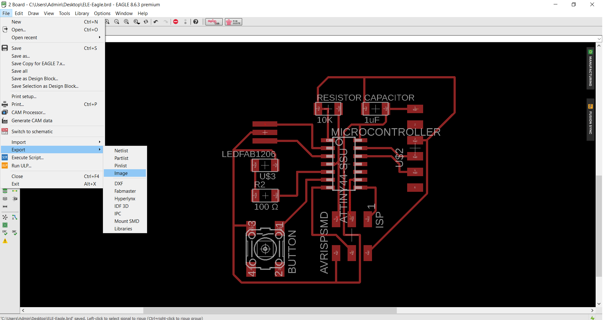
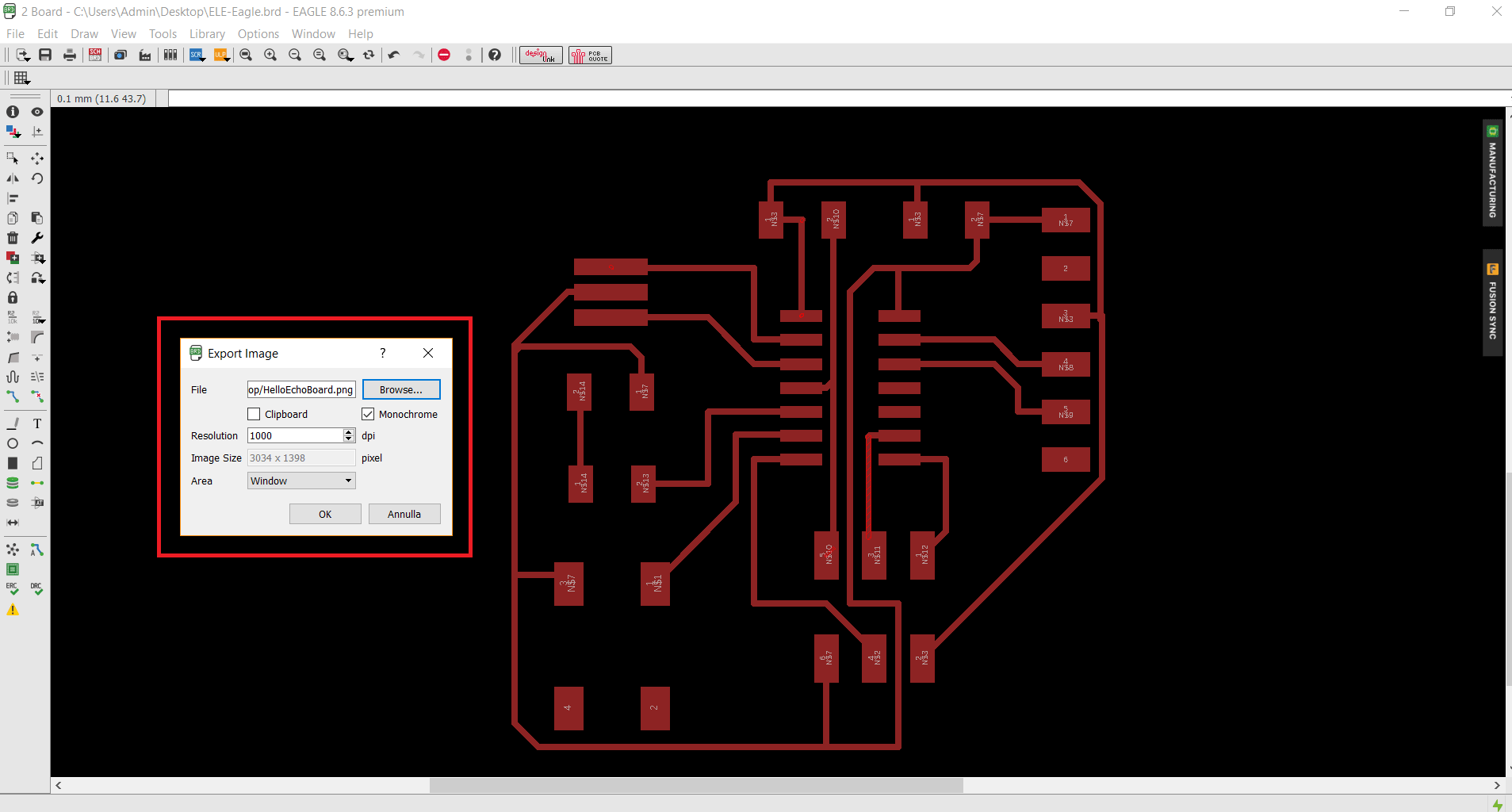
Then, I exported the the image, selecting the Window area and 1000 dpi. Next, I clicked on layers and I selected only the top, because I was interested only on it. Finally, I opened the exported image on Gimp.
Export the board with Gimp
I had some problems with Gimp. Honestly, I think it's a complex 2D modeling programm. I used it to create the .rml files (included traces and outline). As you can see, I added two new layers: the first one was white and the second one was black. They should be useful to create an edge around the traces and to export two different pictures from the main one.
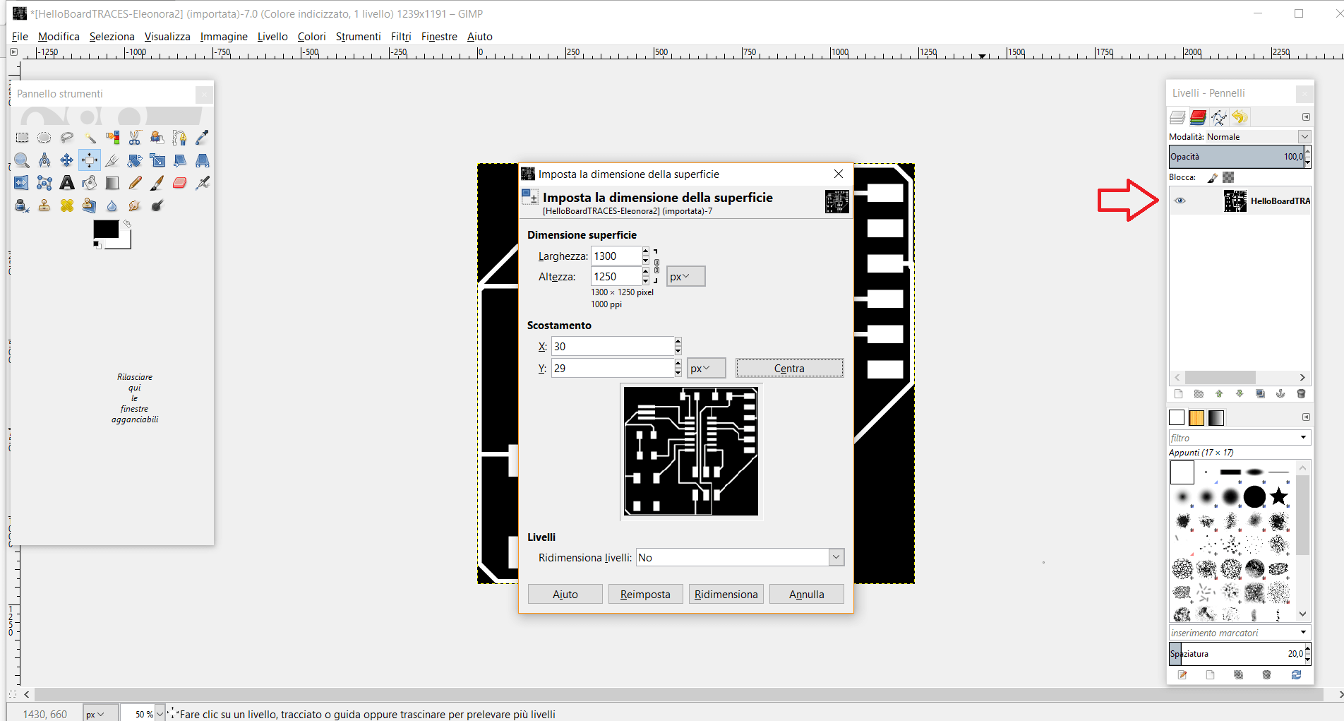
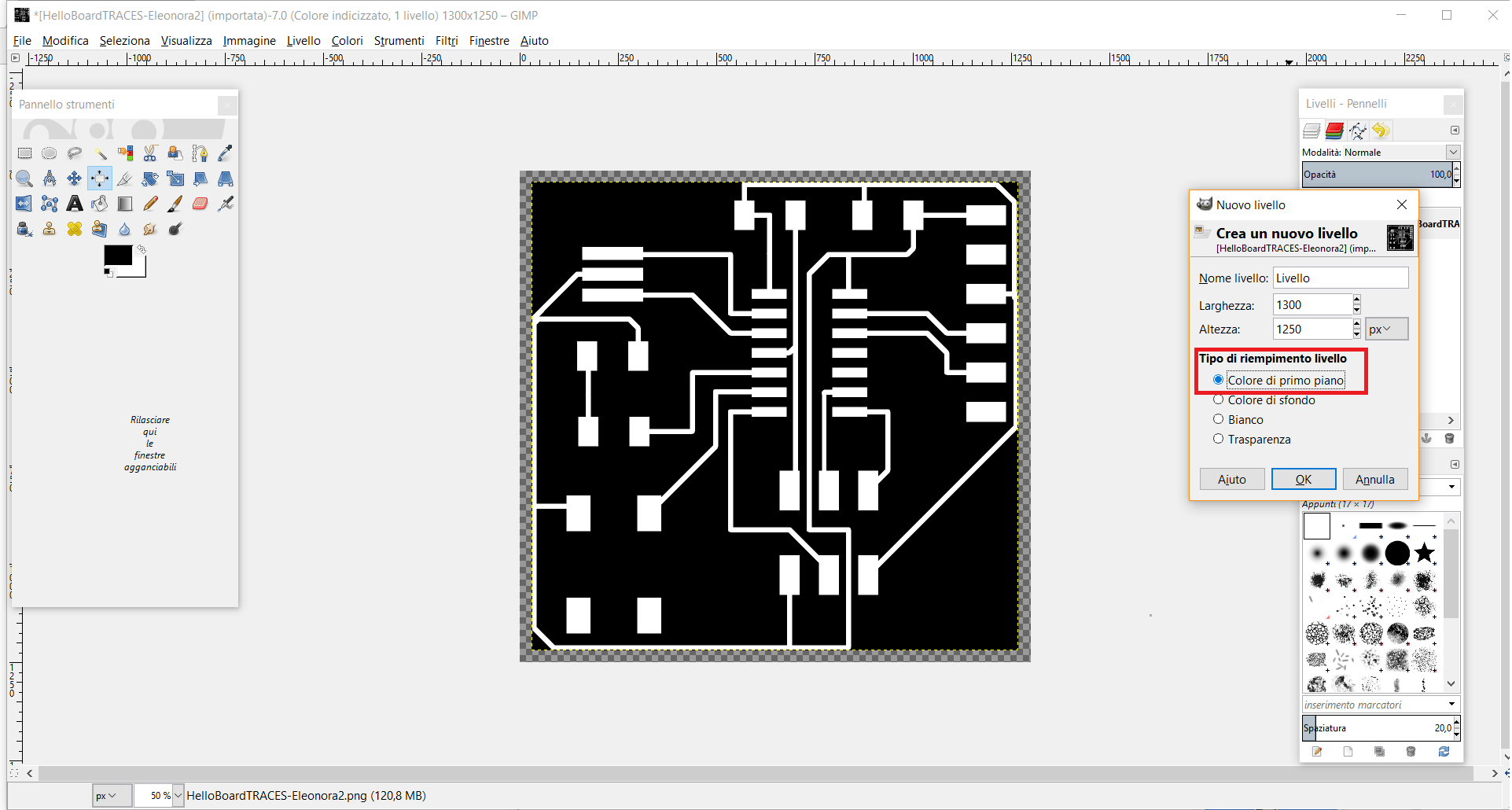
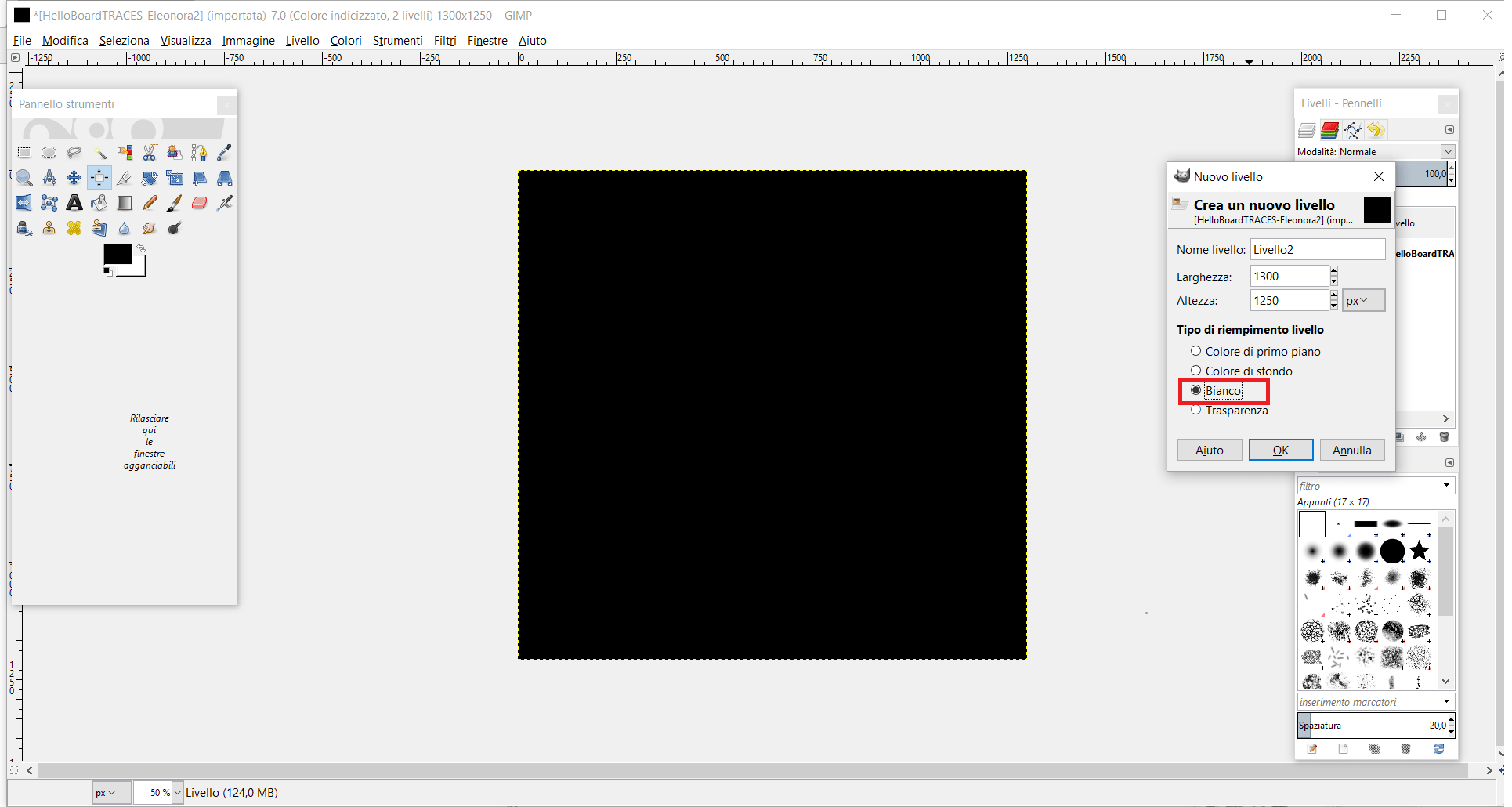
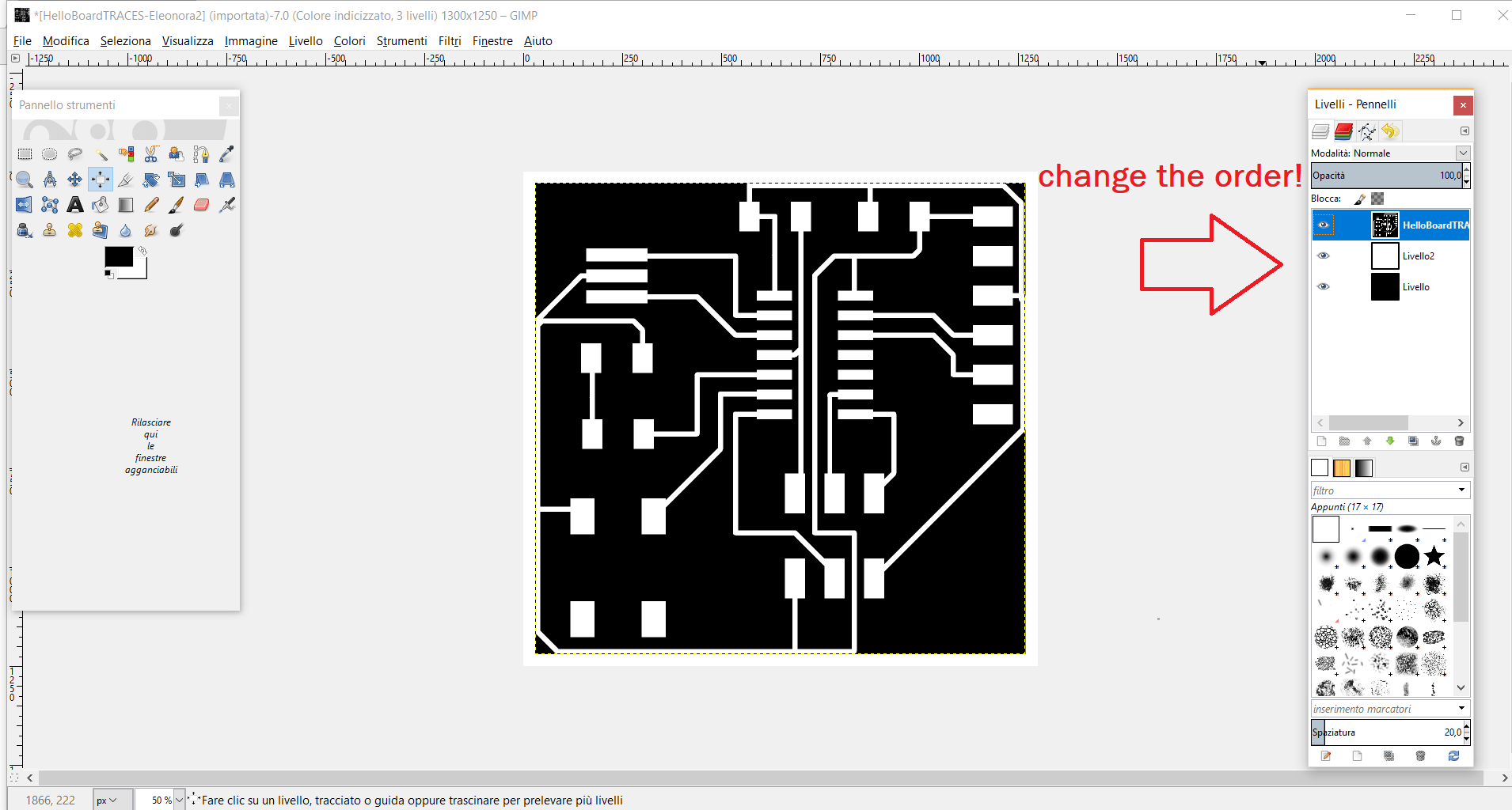
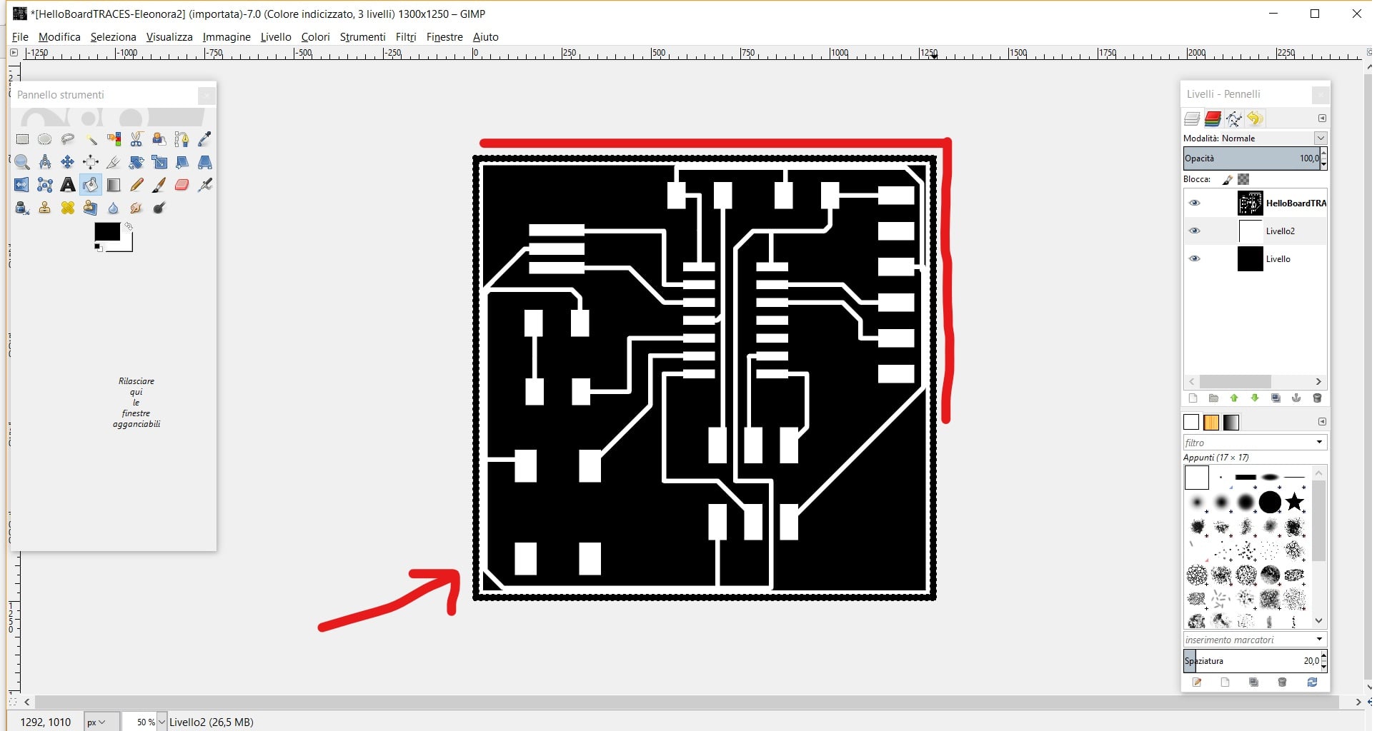
I resized the dimensions because the area near the traces was too large. I saved the image clicking on Maiusc + Ctrl + E. Then, I did the same thing to create the outline. I inverted the colours, setting up the white as the main one. But, as you can see the edge between the traces and the outline is too near to my traces. So, the board will never work! I decided to repeat the steps and finally I obtained a good result. I will update this small part with the last two or three screenshots.
So, after having done my edge, I saved the image of my outline. Finally, I followed the same passages used during the electronics production's week and you can transform the .png file in a .rml one and you can mill your board (1/64 traces and 1/32 outline) with the Roland Machine.
Bill of materials (BOM)
At this point I began the tour into my FabLab looking for the hello board components.
The table below shows all of them (included the led, the button and the restistor I decided to use).
| COMPONENT | QUANTITY |
| ATtiny44 | x 1 |
| Resonator 20MHz | x 1 |
| Resistor 10K | x 1 |
| Capacitor 1uF | x 1 |
| FTDI | x 1 |
| ISP | x 1 |
| (+)COMPONENT | QUANTITY |
| Resistor 100 ohm | x 1 |
| Button | x 1 |
| Red led | x 1 |
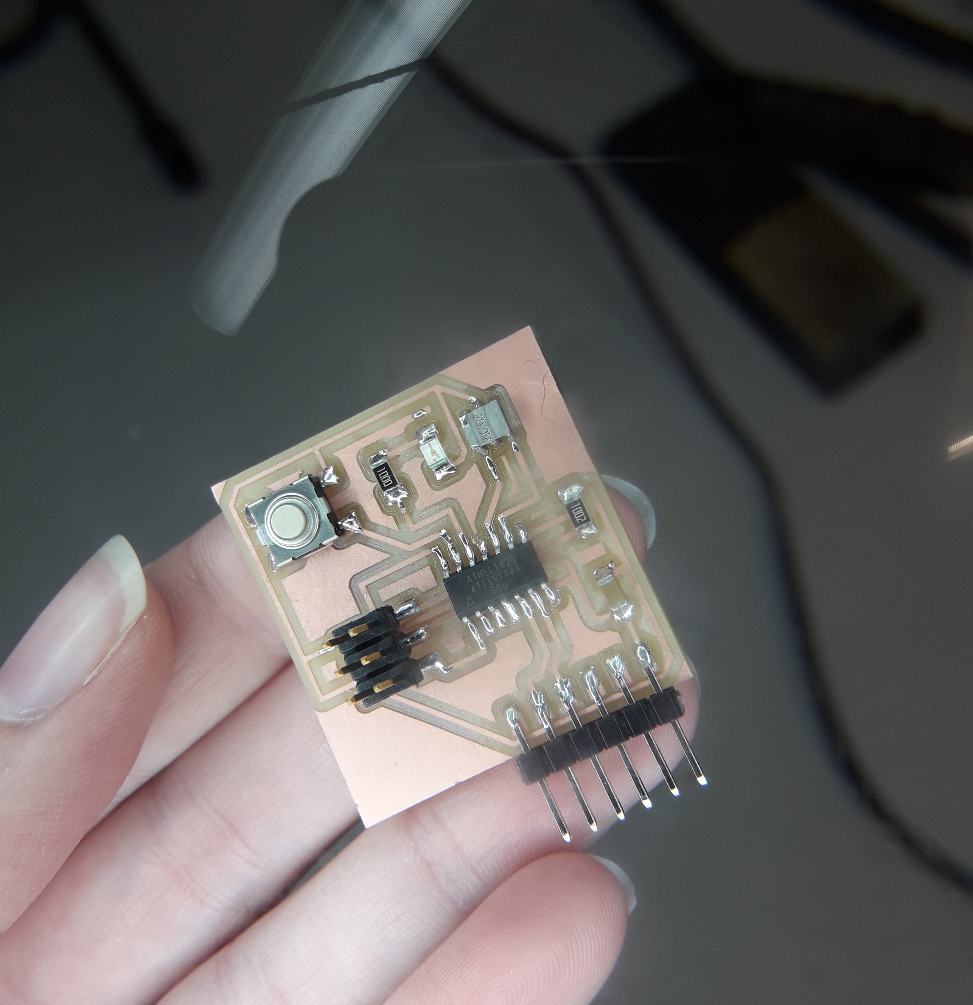
Milling and soldering
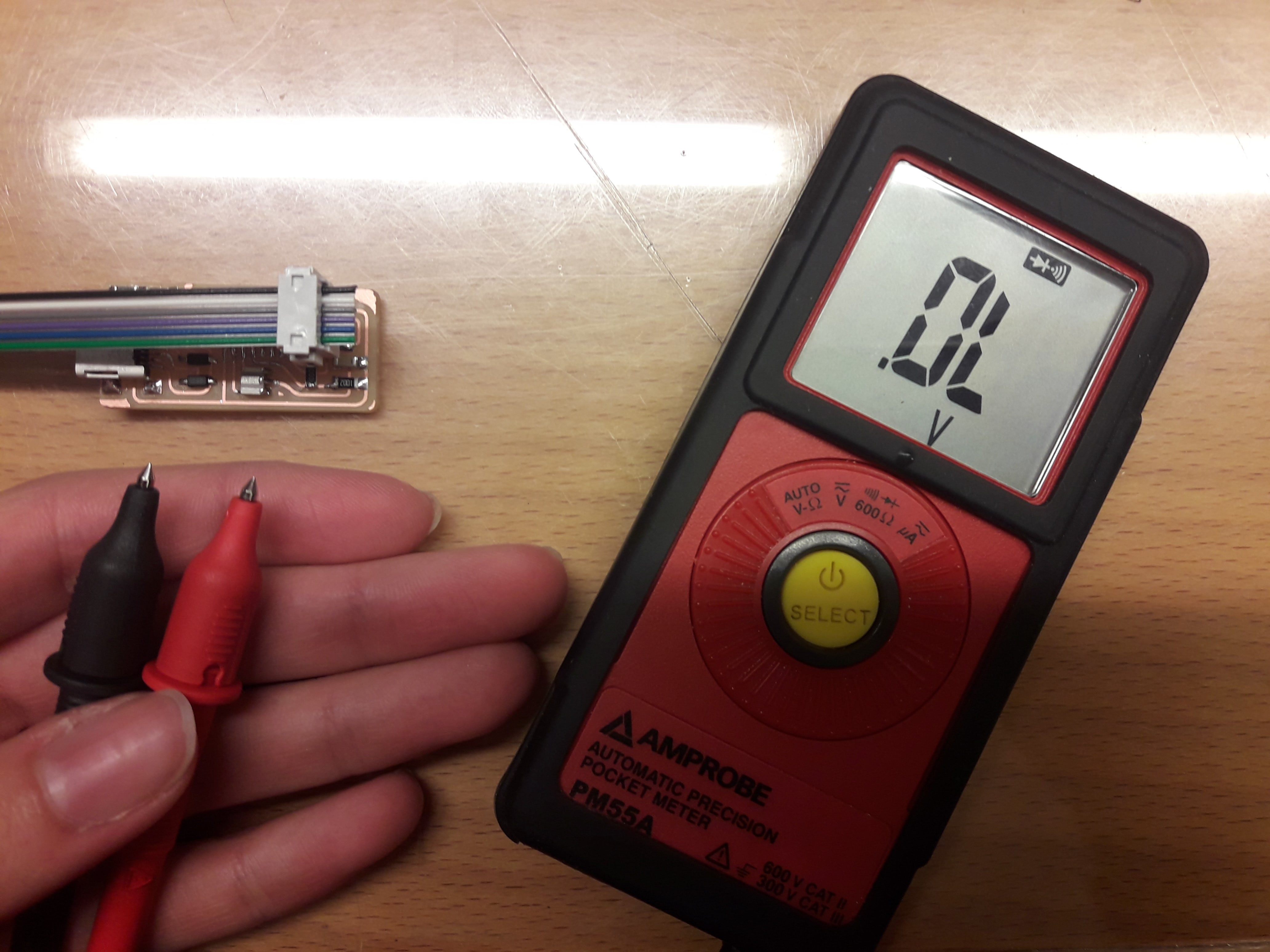
Finally, I started soldering. Obviously I put the board's image in front of me and it helped me a lot (considering the fact I'm a beginner). In addition, I had a doubt about the red led I decided to use. So, I asked to Simone how can be sure about the cathod and the anode positions. He explained me the negative part should be have a thin green line, but thanks to the use of a power supply I learned that the black cable is the negative part and the red is the positive one. After having set the Channel 1, we put the values for the Voltage and for the Ampere. Then, I put the led on the table and I linked the green line to the black cable and at the same time, I linked the red cable to the other side of my led. I noticed that the red light switched on. Thanks to this kind of test I had the confirm the green line represents the negative part.
Conclusions
Even if it has been hard, I liked this week's assignment. After our Italian review, I would like to redraw the board again, changing the components position and using a larger thickness for the traces. In addition, I noticed I put the ATtiny44 in the wrong position. In fact, I put the VCC on the right side at the bottom. After, this week's failure, I will try to do the soldering again and I'm sure I'll remember this thing for the rest of the next months!
That's all! I have to work really hard!
Useful links:
Fab Academy's archive - Electronics Design (Eagle)Jacksoft Labs - How drawing a PCB on Eagle
Creating parts (tutorial by Adafruit)
Importing/Adding a new library
Routing the board
