Week assignments
Group assignment:
- Send a message between two projects (assignments made by different students)
Individual assignment:
- design, build, and connect wired or wireless node(s) with network or bus addresses
Group assignment
You can find documentation about our group assignement on our group page.
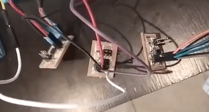
My I²C communications trials
For this week, I wanted to win some times by using my already existing boards from input and output devices. Instead, I lost a lot of time troubleshooting what didn't work at the end. The reason why I didn't succeed in my opinion is that I tried to use boards not designed at first for networking and communications. Here is a list of problems I experienced :
- MOSI Pin from LCD board was already used by the LCD so it can't been used by both LCD and SDA.
- I had Tx/Rx pin from FTDI using MOSI so it it can't been used by both LCD and SDA.
- Input board was burnloaded at 8MHz and Output board used an external 20MHz. FTDI was not responding correctly anytime I powered them together.
- I didn't have dedicated SCL and SDA pins so I used AVR pins which was requiring a lot of pluging and unpluging and wiring on a breadboard.
- TinyWire libraries where inconsistent. I downloaded 3 libraries : - TinyWire, - TinyWireM and - TinyWireS. I wanted to use only TyniWire at first since it can be used for both master and slave. At the end it appeared that I had improvments using dedicated libraries for master and slave. I also had to correct examples to have it work on my designs.
Also, didn't visualizing the difficulty correctly at first, I started with the most difficult challenge : Printing on the LCD "Button pressed".
At the end I was able to use the input board as master with an arduino as a slave and the ouput board as slave with an arduino as a master.
I wonder if the clock speed can have something to play in it since at the end I tried to burn my two microcontrollers with 8Mhz internal or 1MHz internal. None of them worked.
I will not try anymore to connect them since I realised that is not the way it should be done and there is too much room for errors.
My hello.bus.45 exercice
Doing this exercice took me less than 5 hours from milling to proof of concept. This should have been the time used for this week assignement.
Building and wiring
I used directly neil's traces. My workflow was the following :
- Using imageToGerber utility to convert neil's traces
- Readying the job in Flatcam
- Milling my boards
- Soldering the components
- Uploading a blink program to check boards functioning
- Wiring on the breadboard since I don't have IDC bus connectors
Coding
For coding I used directly Neil’s code modifying only line 41 for nodes board with ‘1’ and ‘2’ instead of ‘0’
#define node_id '0'Below is a copy of the main loop:
//
// main loop
//
while (1) {
   get_char(&serial_pins, serial_pin_in, &chr);
   flash();
   if (chr == node_id) {
      output(serial_direction, serial_pin_out);
      static const char message[] PROGMEM = "node ";
      put_string(&serial_port, serial_pin_out, (PGM_P) message);
      put_char(&serial_port, serial_pin_out, chr);
      put_char(&serial_port, serial_pin_out, 10); // new line
      led_delay();
      flash();
      input(serial_direction, serial_pin_out);
      }
   }
}
It takes as input any character send through serial.
If this character is a node id then it flashes all the leds once and the given node led twice.
It also write back into the serial monitor "node 'id'"
Here are the videos of the result. The first one is the boards side, the second one is the serial monitor side.
As you can see, the serial monitor didn't return correctly "node 0" and "node 1". I didn't find how to fix it. It might come from a loose cable.