Week 5. Electronics production
The main objectives were to characterize the design rules for your PCB production process and to make an in-circuit programmer by milling the PCB and also program it.
fabricating the PCB
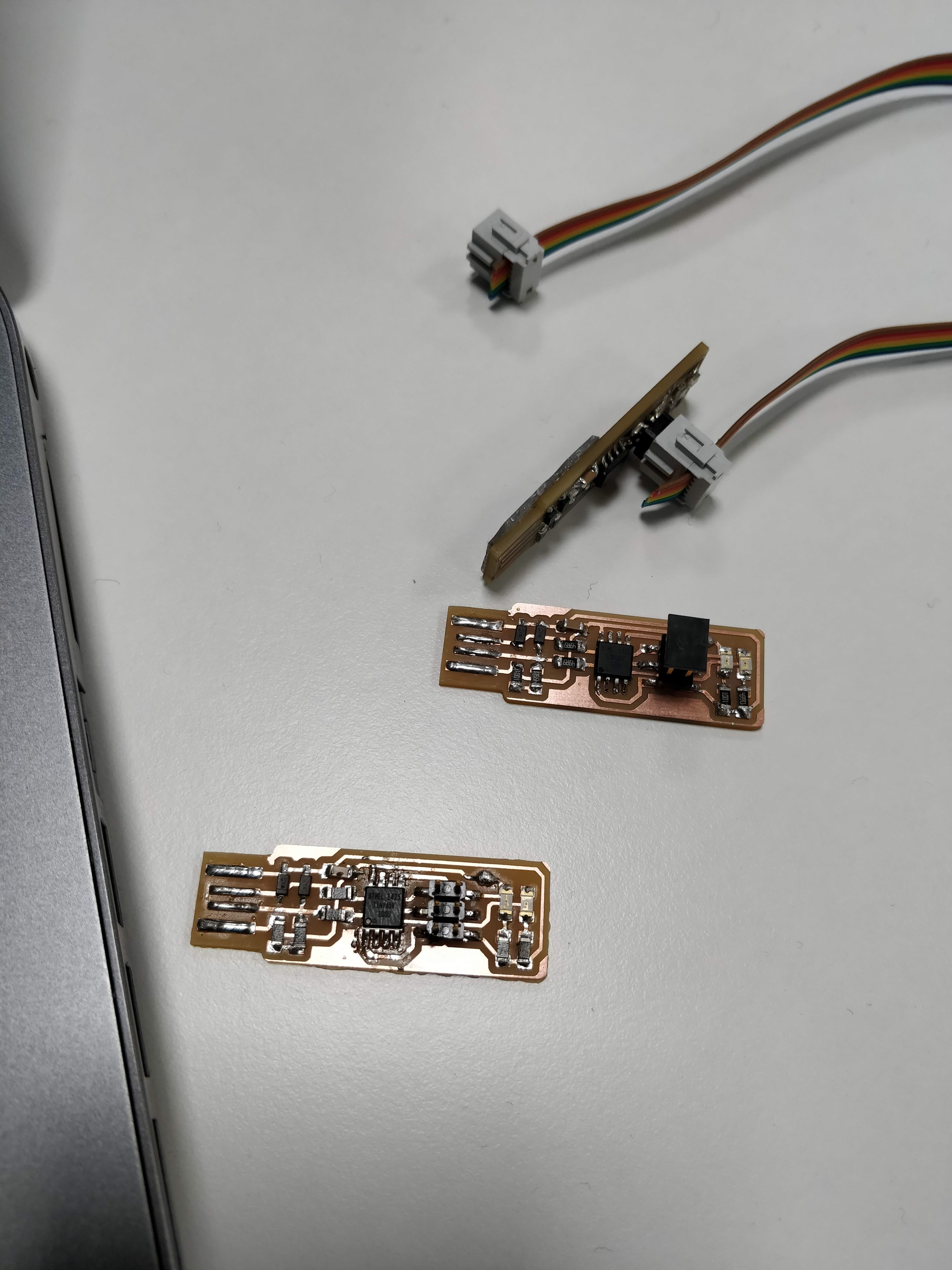
For the given objectives, the designing of the programmer board is not required but it is required to mill and solder the board from the given design. After going through the design suggestion list by Neil I decided to work with the design made by Brian.
Generating the milling files
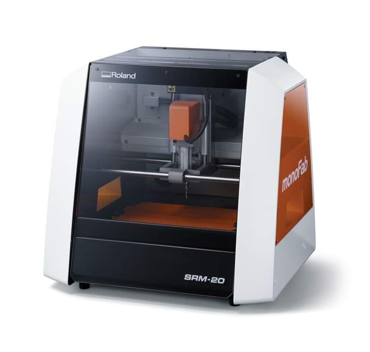
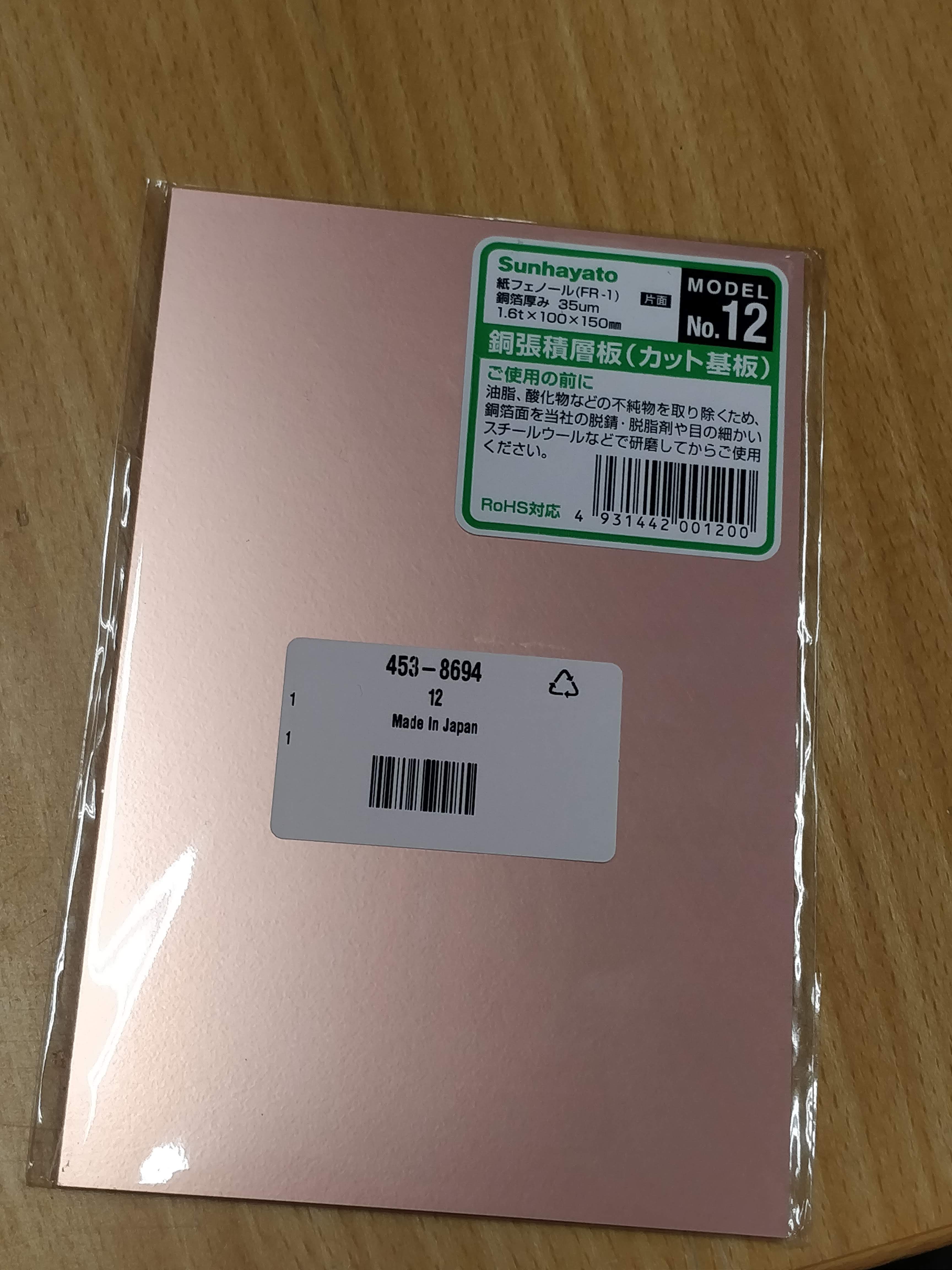
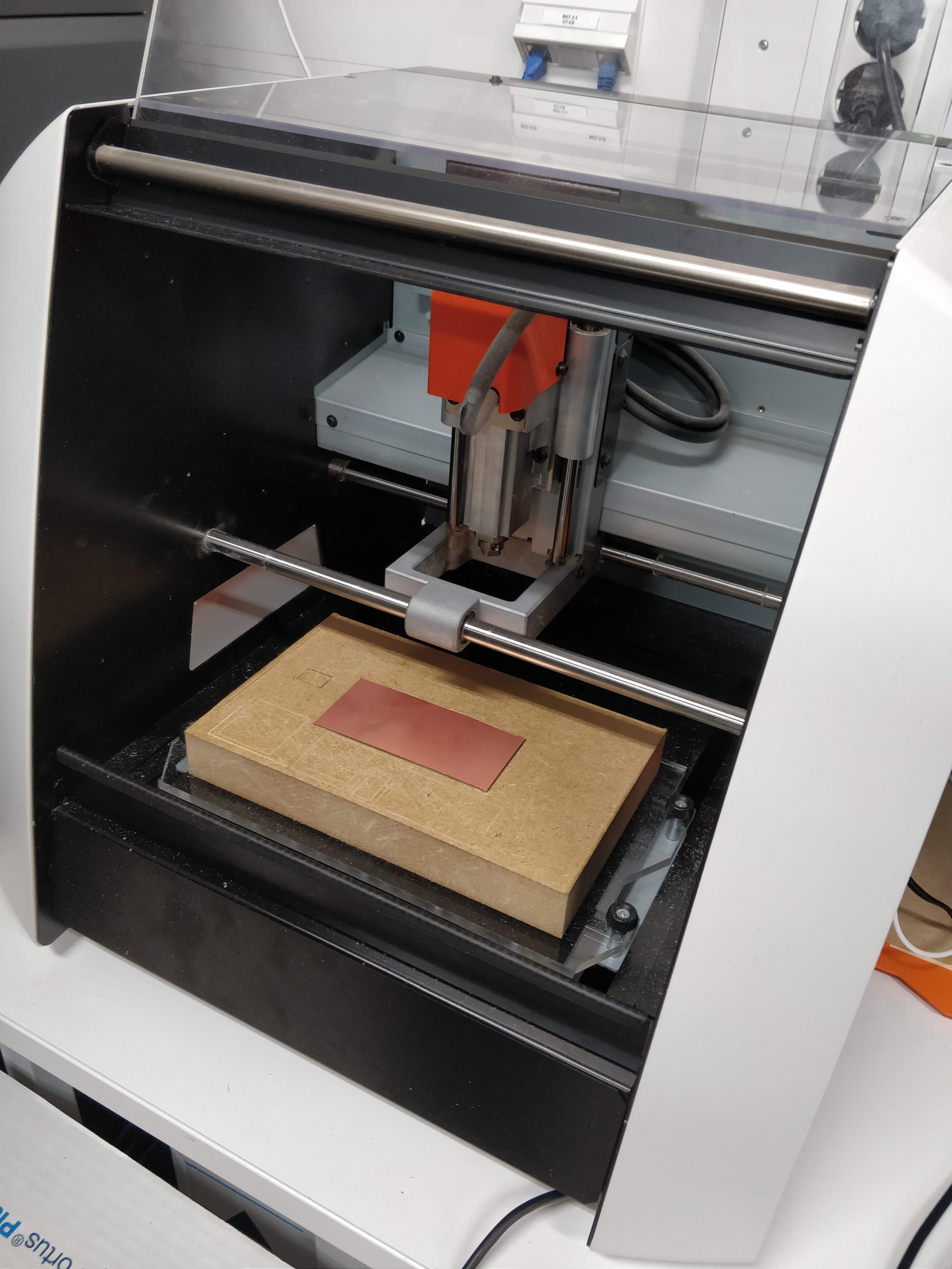
Fablab Oulu uses the Roland SRM-20 CNC milling machine and I have used it to mill the PCB in an FR-1 board. Therefore it is required to use .rml files. To begin with, .png files containing the traces and the board external cutout were downloaded from Brian's page. .
To create the .rml files I have used the fab mods . First, select the program and open server program from the left top menu. Next, select the Roland SRM-20 PCB from the list. Then it will automatically open a page with different windows.

After that upload the png file which we need to convert. Note that we need to upload a picture with more than 1000 dpi here.From the second window (PCB default) select that mill outline or mill trace option accordingly. The milling is used to mill the traces with the mill bit and outline is used to make the outline and cut the board.
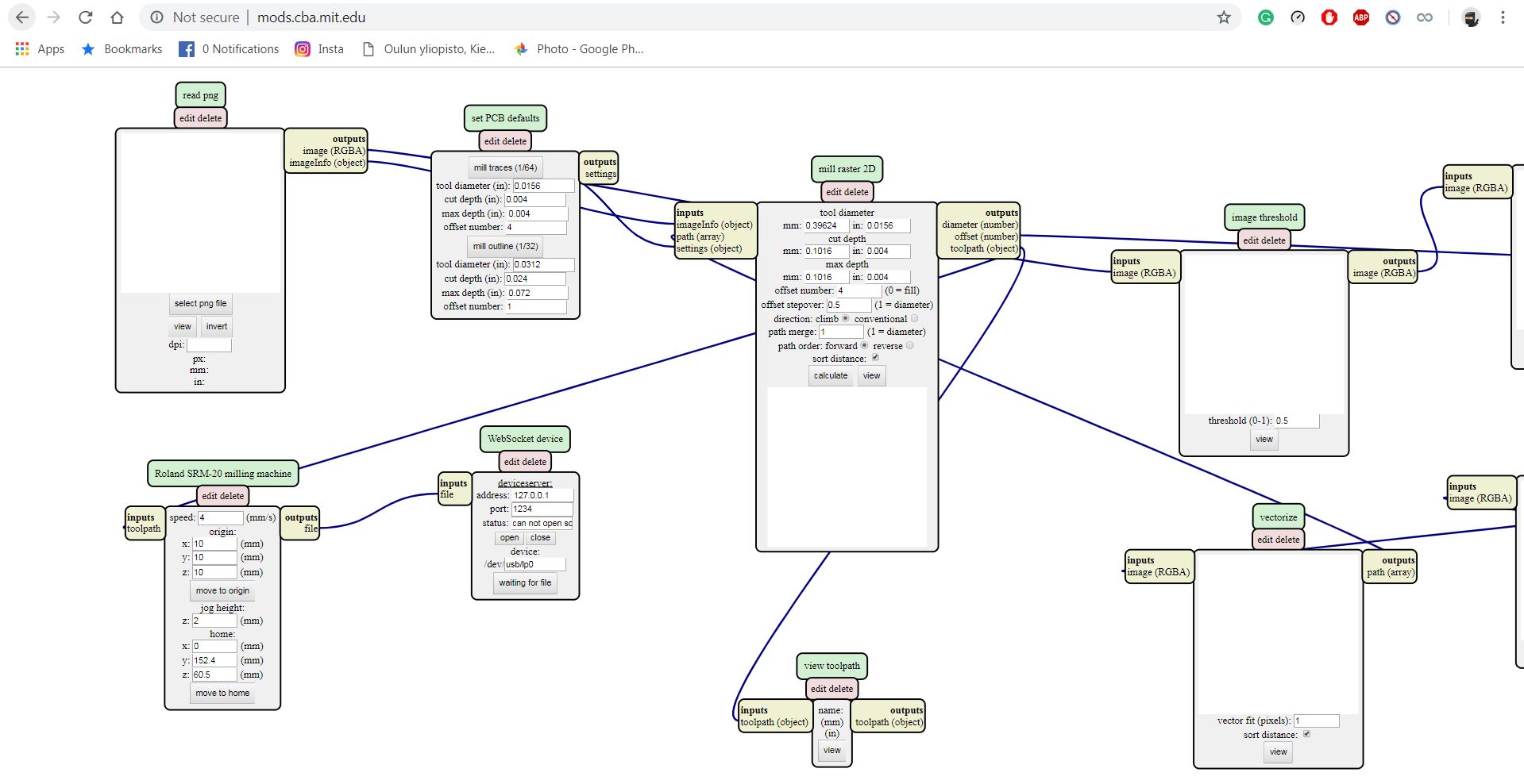
In the next window (mill raster 2D)give the tool diameters and cut depth as required. I used 0.4mm mill bit for milling and 1mm bit for outline. From the Roland, SRM-20 window remove the offset if it is not required.
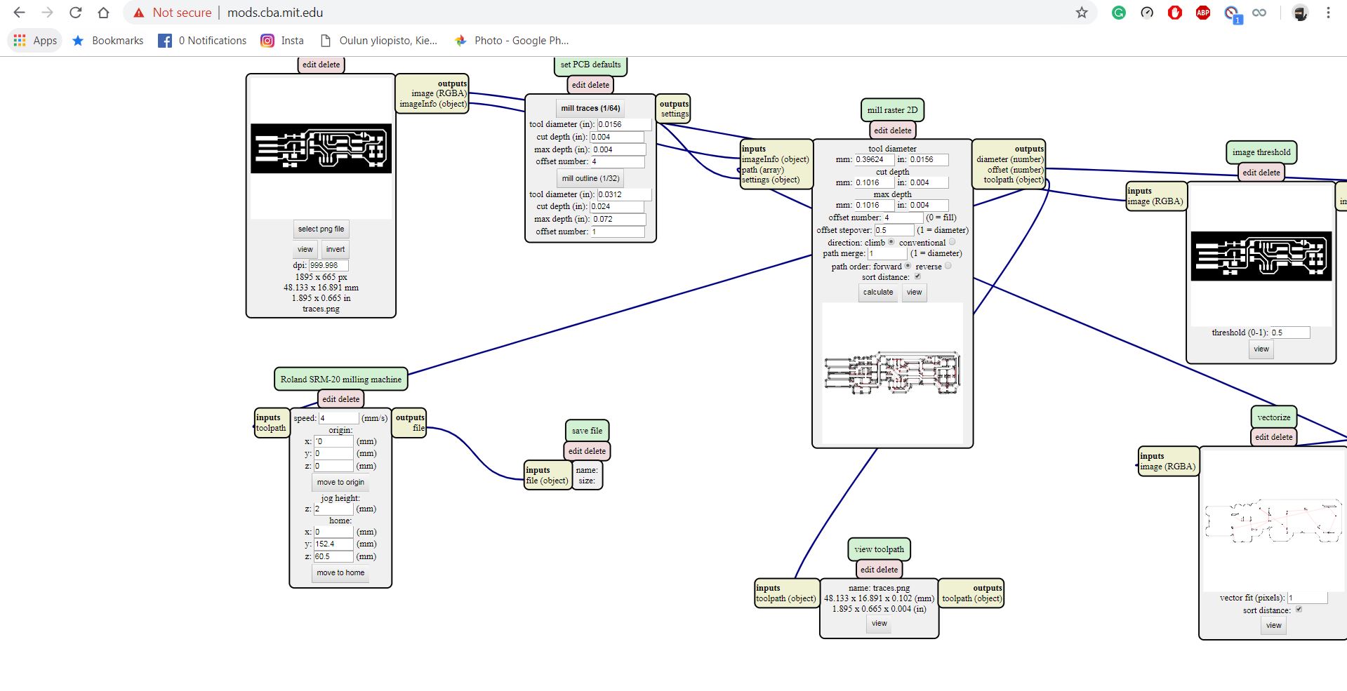
Then delete the next window cascaded and put a new window to save the file by selecting modules, open server modules and save. Then connect the output of the previous window to the input of the save. After that simply then press calculate button on mill raster 2D window and press save the file button on save file window.
Milling process
First, we need to configure the milling machine so that we have to follow these steps.
Open the CNC machine and extract the bottom plate.Stick the board to the bottom board with doubled sided tape and put it back.
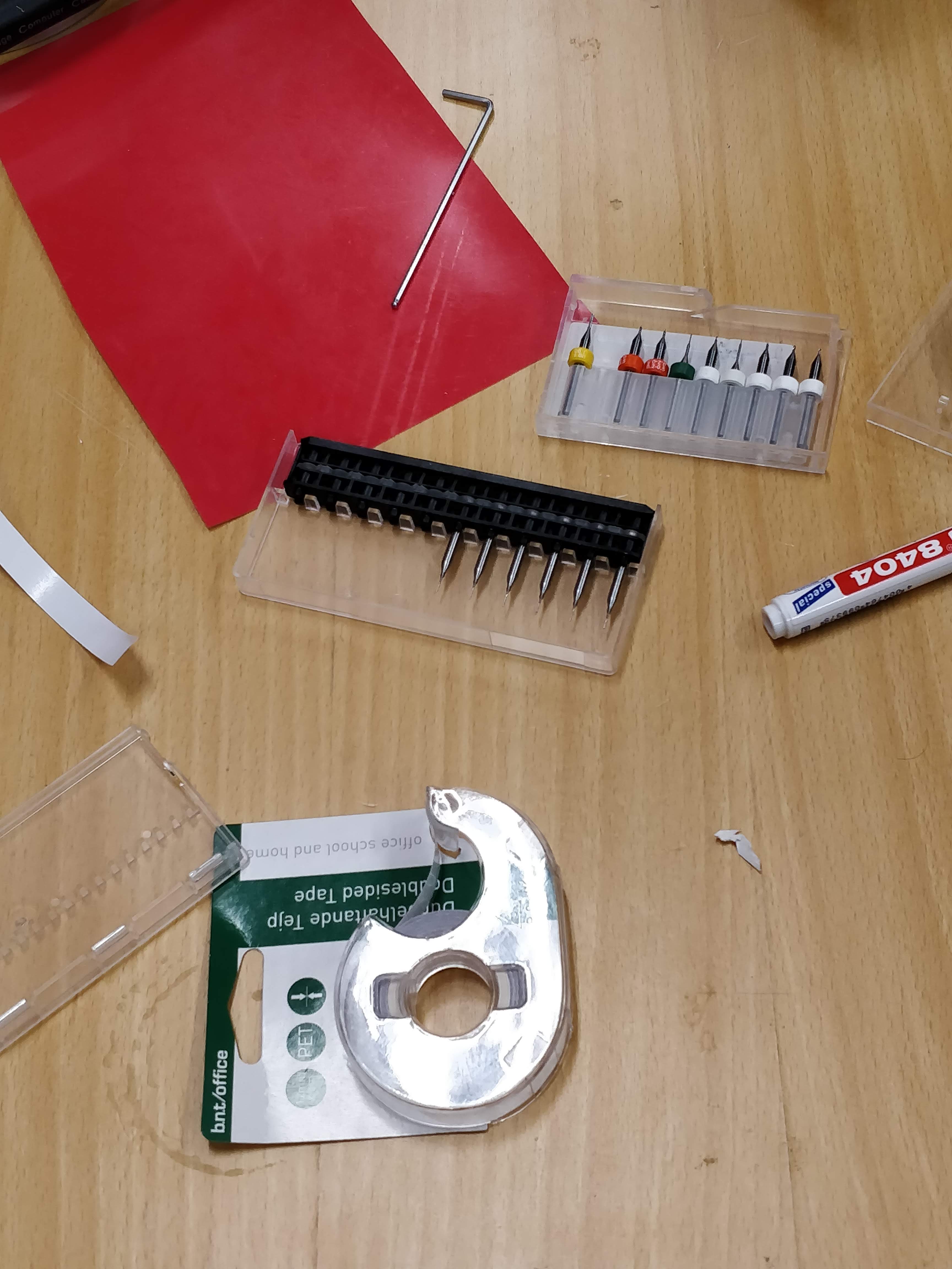
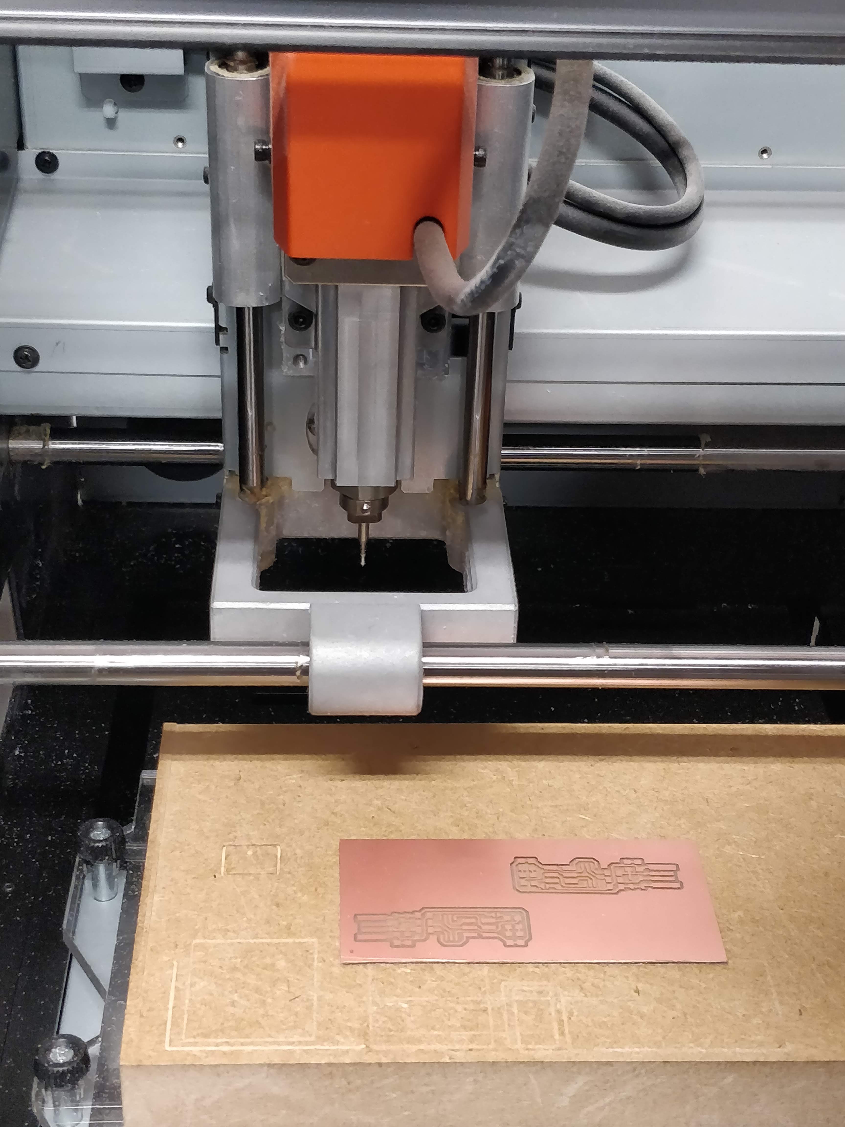
Here I have used 0.4mm mill bit for the traces and 1mm mill bit for the cutting of outline. We need to make the design files according to the mill bits and the PCBs. To insert the desired milling bit into the machine, you need to open the front cover and using your fingers, put the milling bit into its head and tighten it using a hex key. The process of milling using V panel software is described in group work part.
Group Task
For starting the group work we downloaded the files of linetest .png files of linetest traces and linetest interior

We used fab mods to get the file for Roland SRM-20 milling machine and V panel software was used to mill. The steps are presented below.
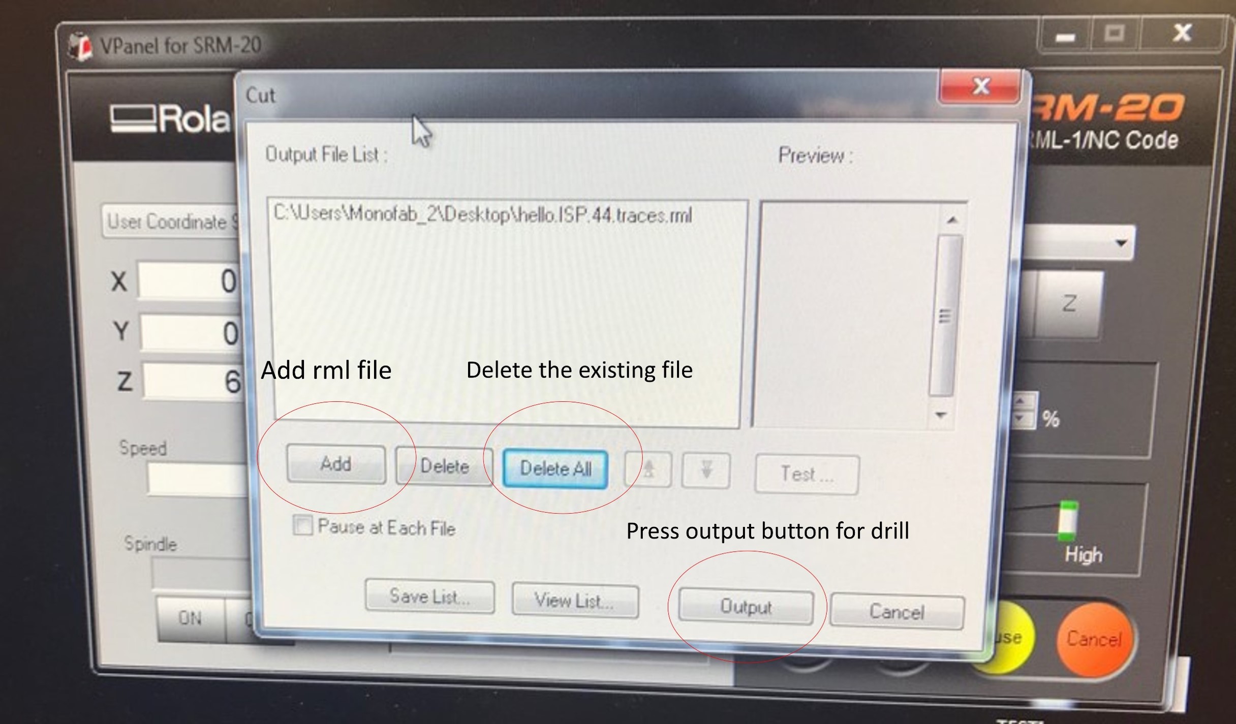
To set the origin pointAfter Opening the Vpanel application in the assigned computer, using x and y buttons go to the point which is wanted as the origin.
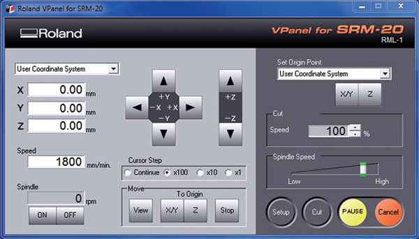
Then set the xy origin by pressing the xy set origin point button on the right top corner. To set the Z origin use Z move button to get closer to the PCB. Next using the Hexagonal Allen tool unscrew the bit enough and touch the mill bit with the PCB. then set the z origin point. Here I have loosen the bit to lower it to the surface of the pcb and then it is required ti re-tighten it before milling.
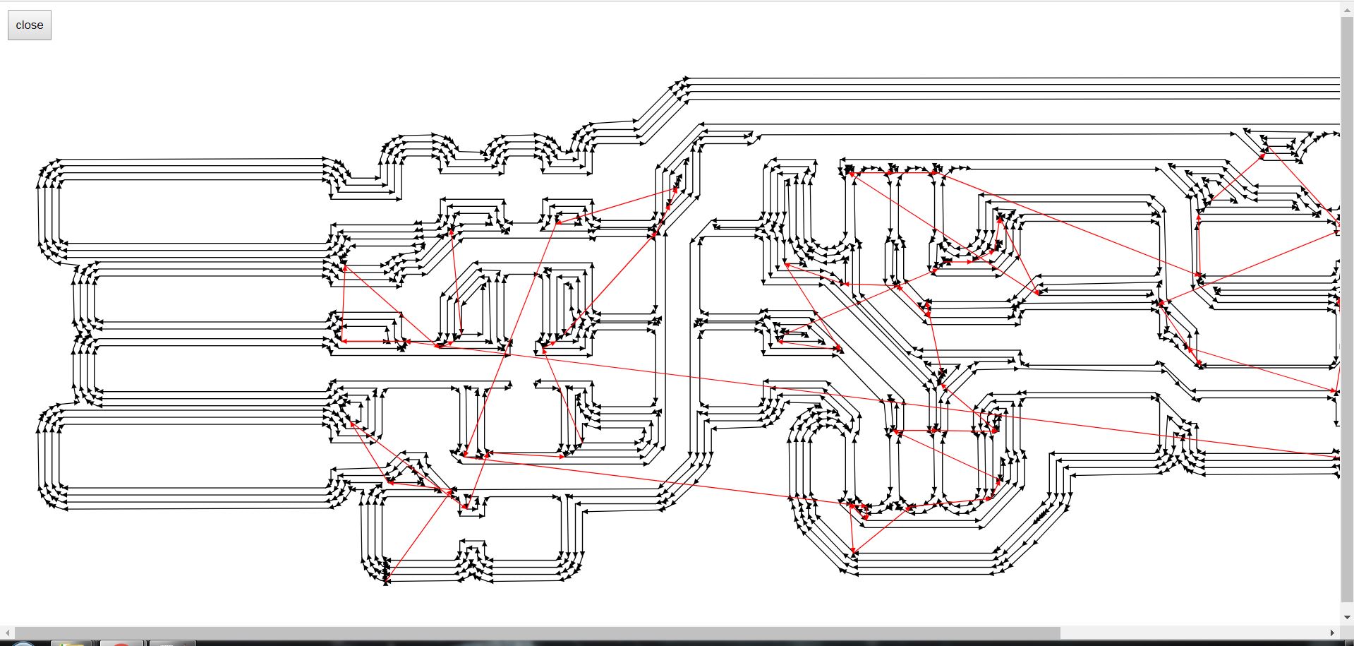
We can start the cutting process by pressing the 'cut' button on the bottom of the window. After that a window will pop up with list of files to cut. Then press Delete All to remove all files in the list and Choose the file that is needed. After that press Output and machine will start milling.
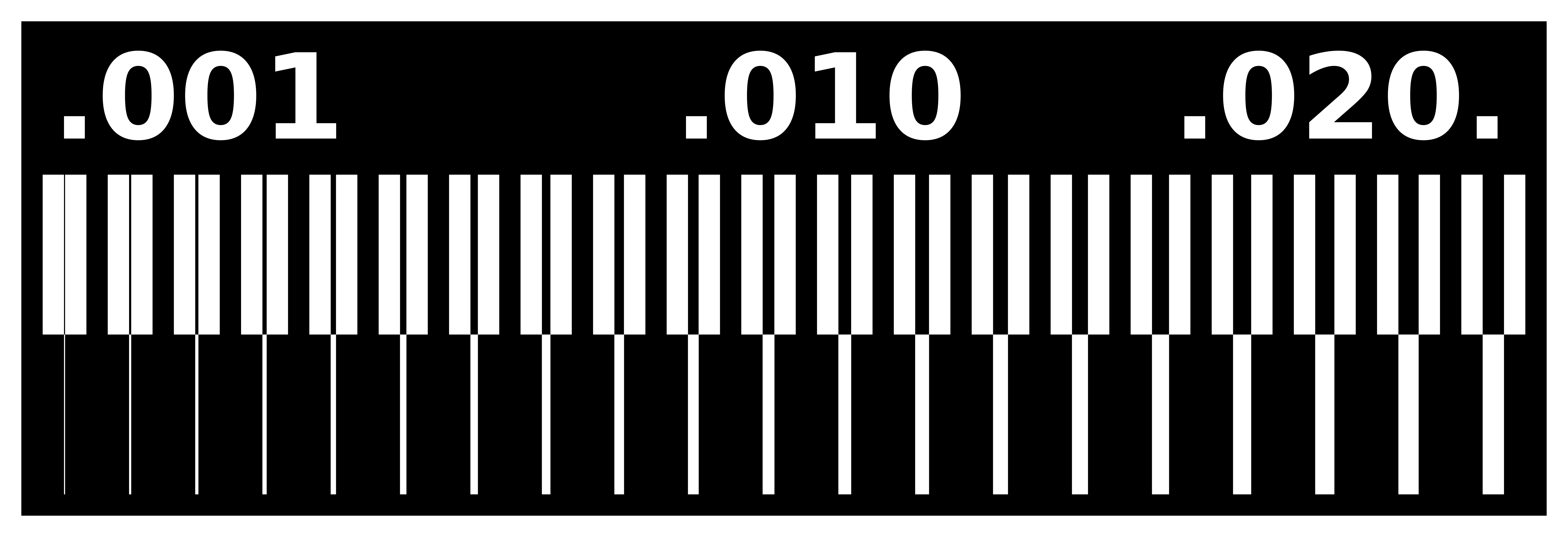
We have used 0.4mm and 0.5mm mill bits to mill the linetest in these, we observed below cuts on the board
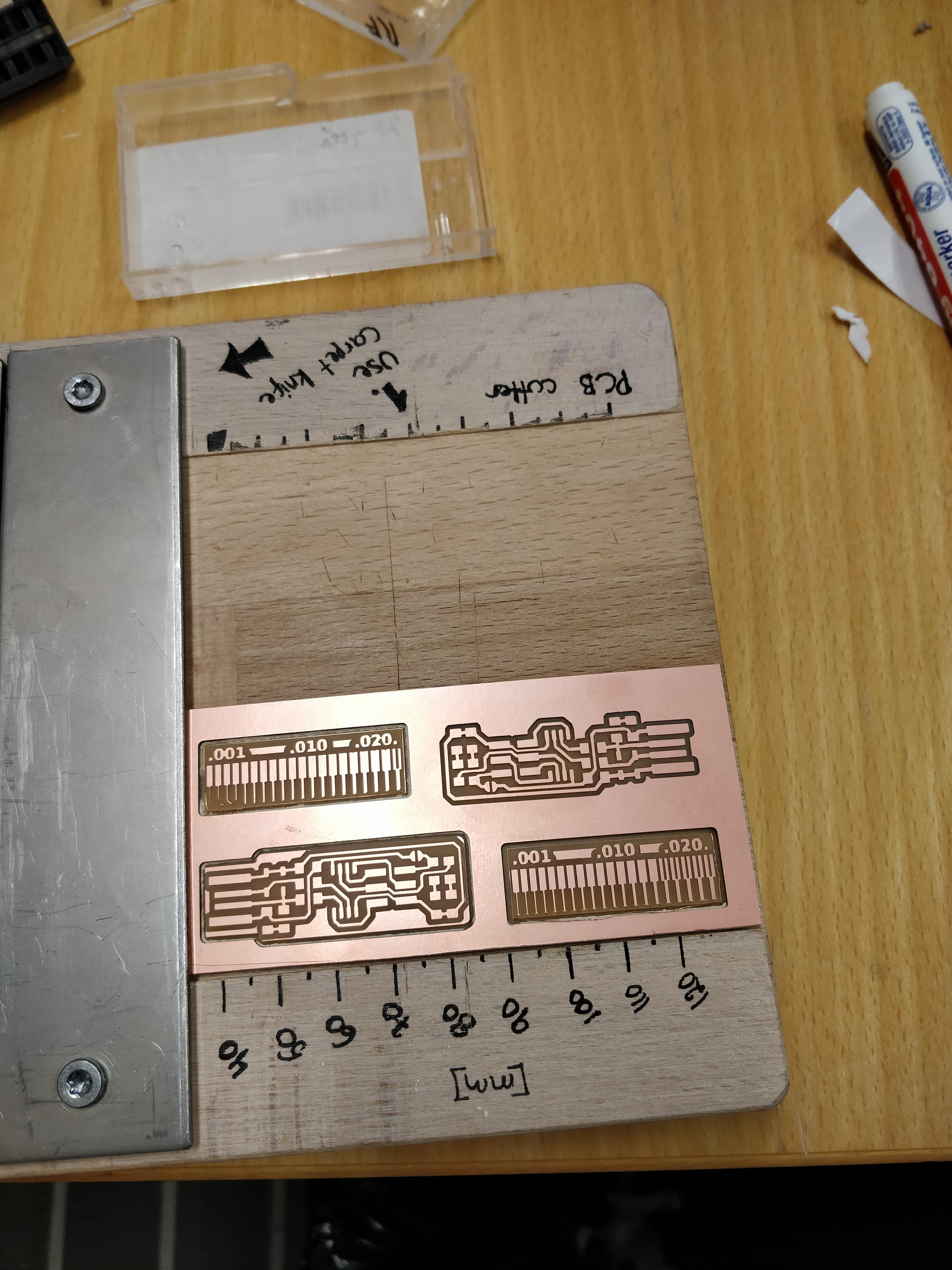
We have used the same board to mill the line test and the two boards to save the area of copper.The top left line test in the picture which was made by 0.5mm mill bit and the bottom right line test was made by 0.4mm millbit. It can be observed that the smallest mill diameter of 0.4mm is able to mill 0.001 mm thicker lines withouut any problem. Therefore it can be concluded that, using the 0.4mm mill bit it is possible to mill the pcb for small details than using the 0.5mm mill bit.
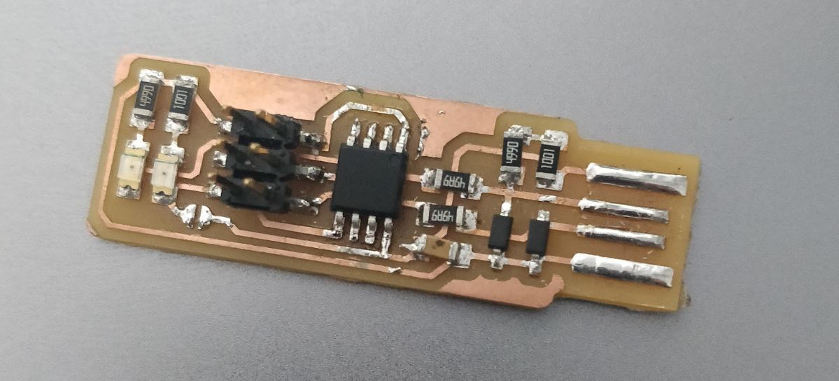
Soldering the components
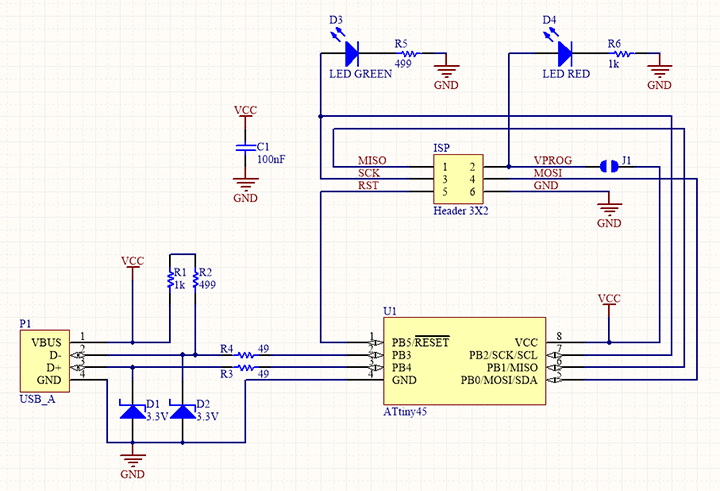
The components needed to solder was listed on Brian's page.
- 1x ATtiny45 or ATtiny85
- 2x 1kΩ resistors
- 2x 499Ω resistors
- 2x 49Ω resistors
- 2x 3.3v zener diodes
- 1x red LED
- 1x green LED
- 1x 100nF capacitor
- 1x 2x3 pin header
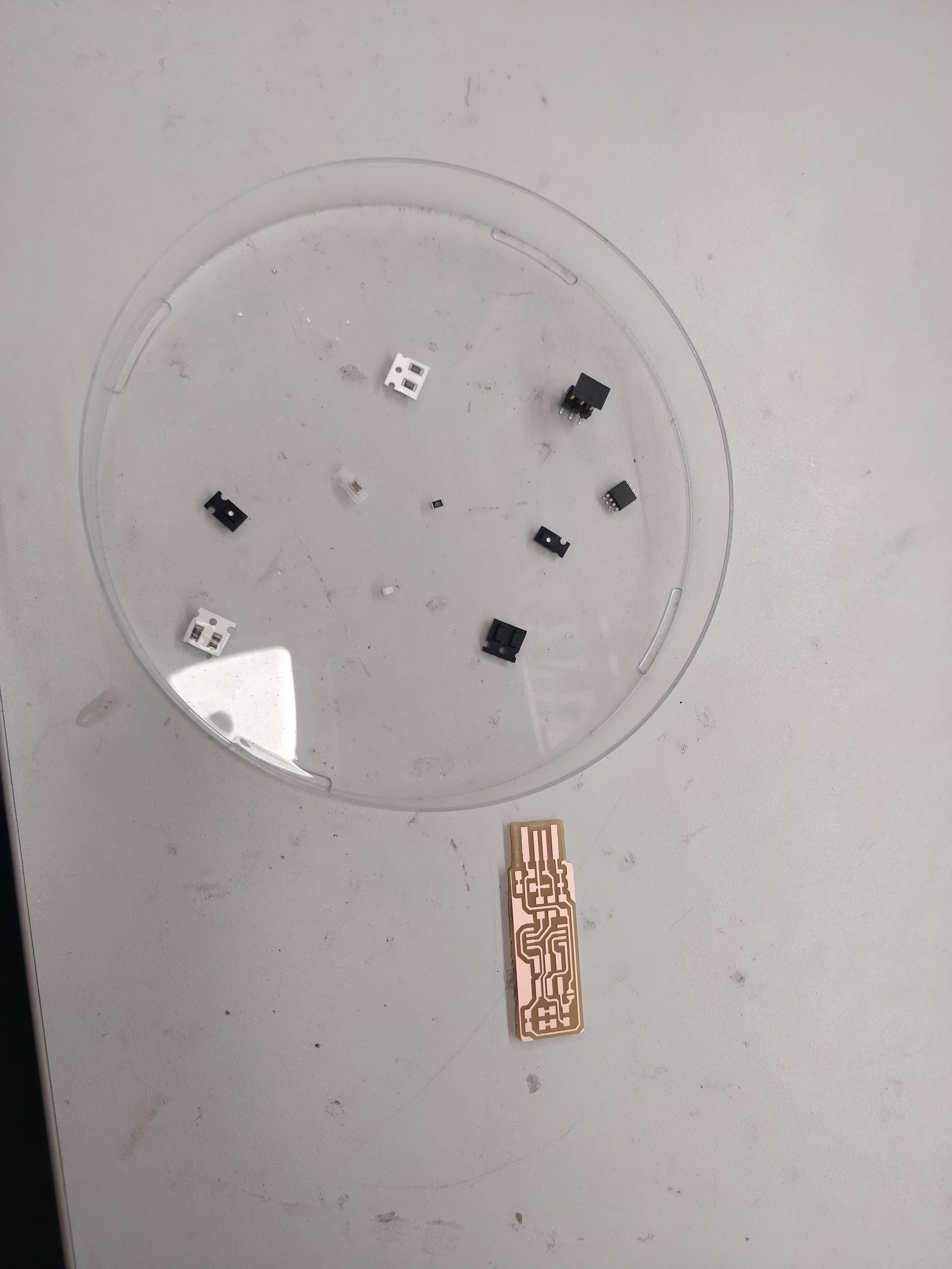
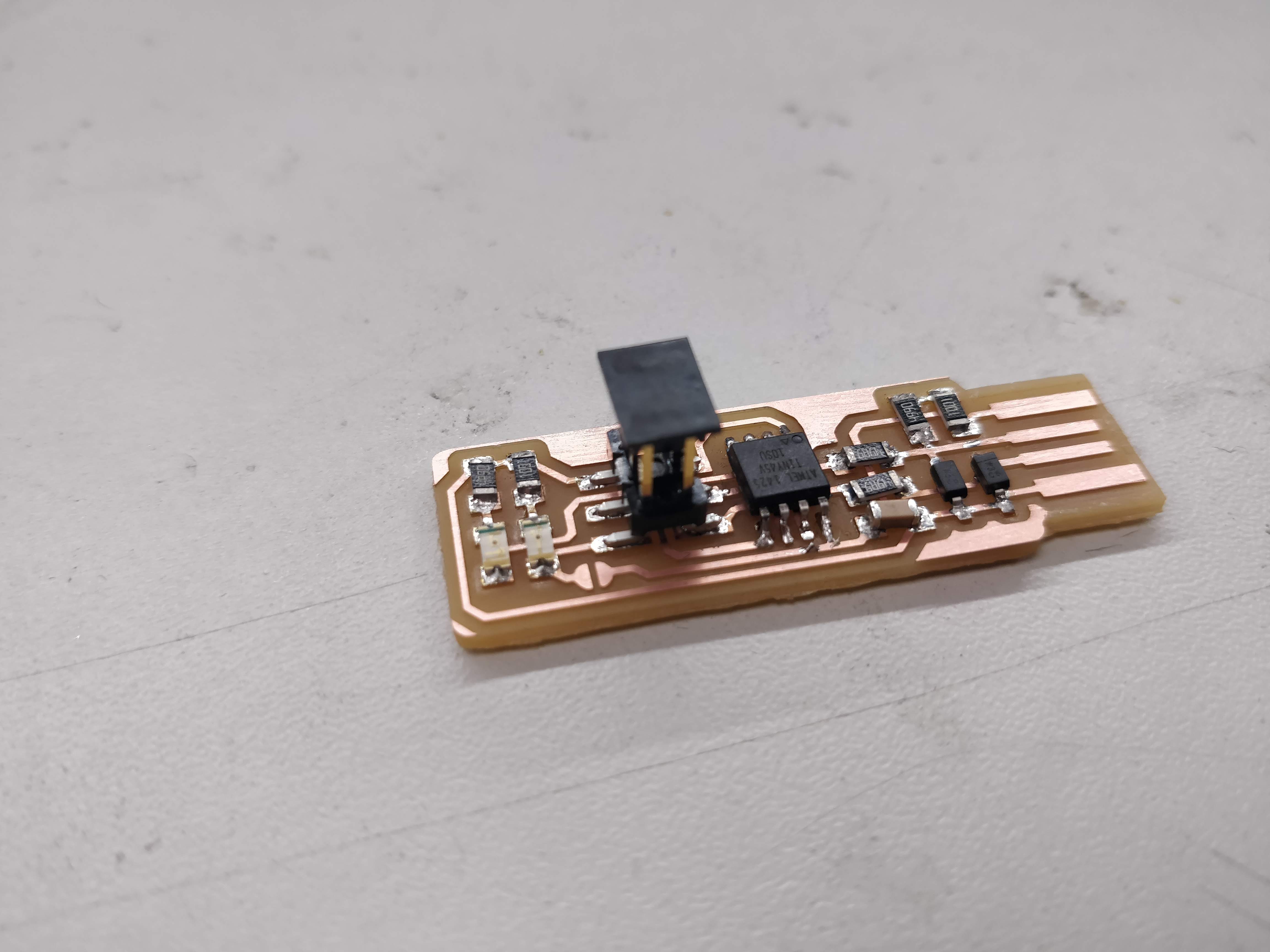
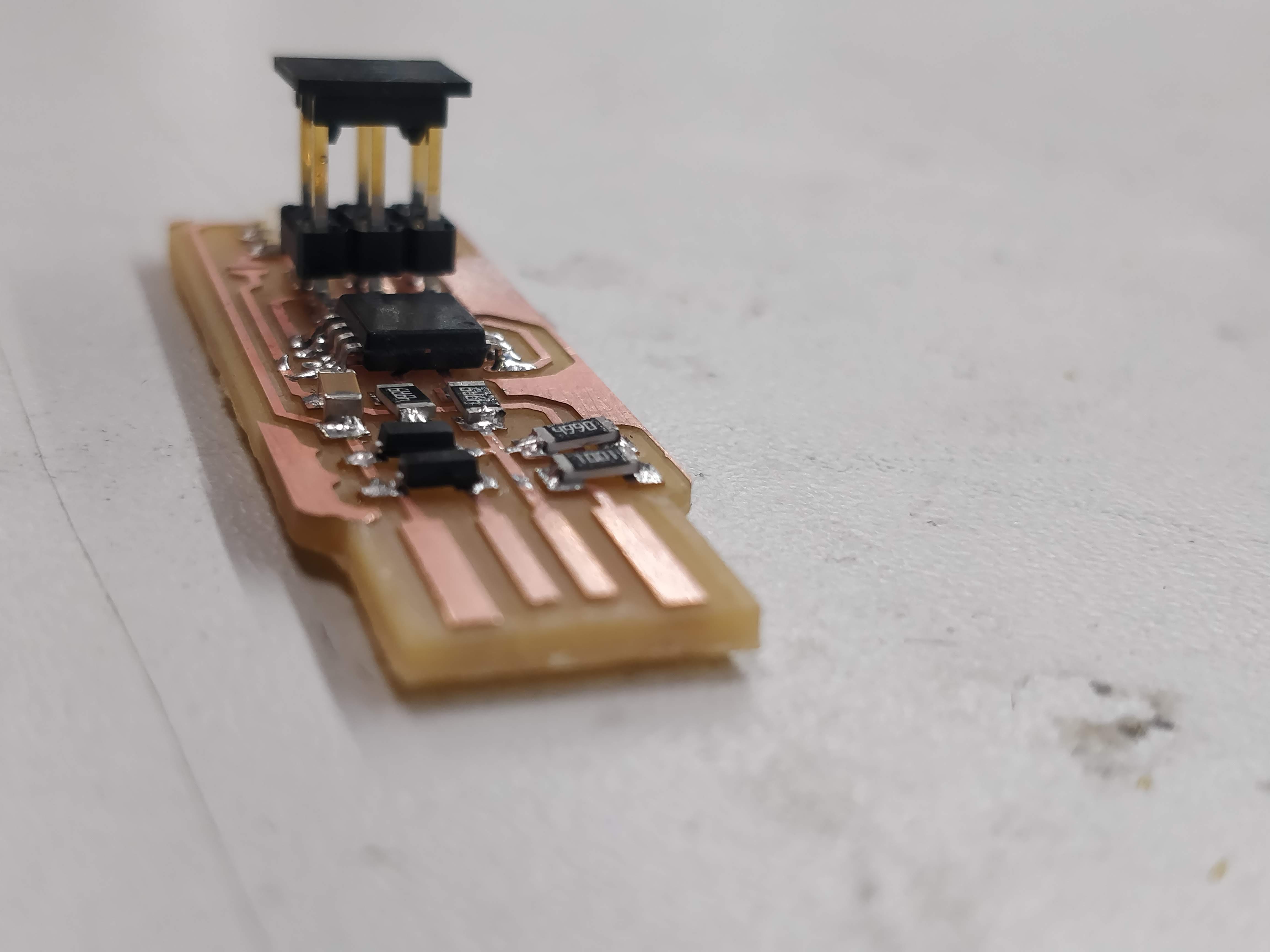
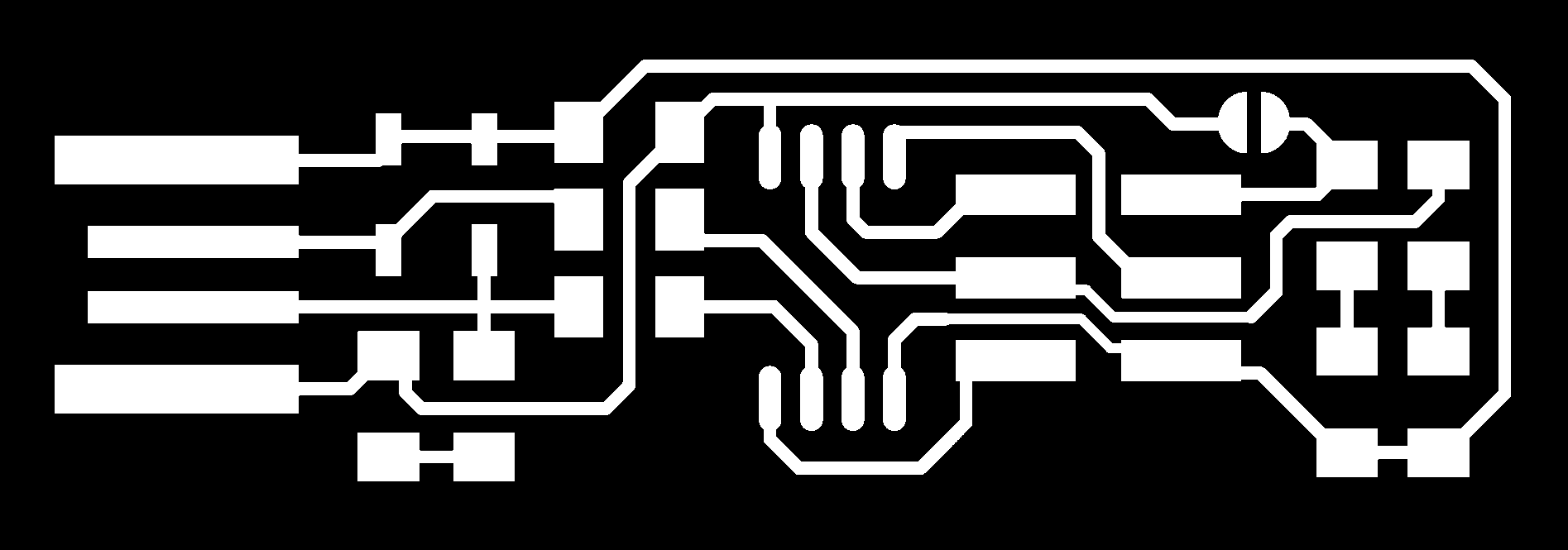
I used the following layout which is given in Brian's page to arrange the components correctly before soldering.
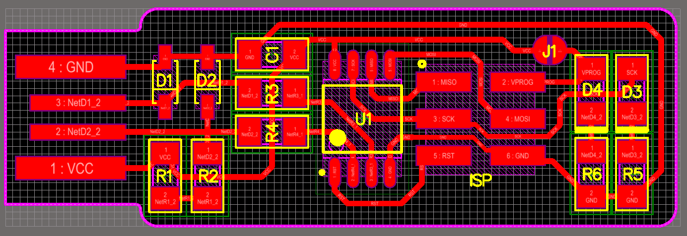
Then I soldered the components on to the milled PCB. The final design after all the components soldered shown below.
programming
Instructions given by Brian's page was closely followed to start the programming after making the programmer. I did the programming on Windows OS, therefore, I had to install Atmel GNU Toolchain ,Gnu Make , and avrdude in addition to GIT. Here Avrdude just needs to be extracted and no need of installing.
Next, I updated the path by going to Control panel -> System -> Advanced System Settings (this will open a new System Properties window) -> Advanced -> Environment Variables button in User variables section.
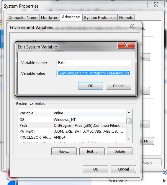
Here I have added these 3 paths by selecting Path Editing.
- C:\Program Files\avr8-gnu-toolchain-win32_x86\bin
- C:\Program Files (x86)\GnuWin32\bin
- C:\Program Files\avrdude
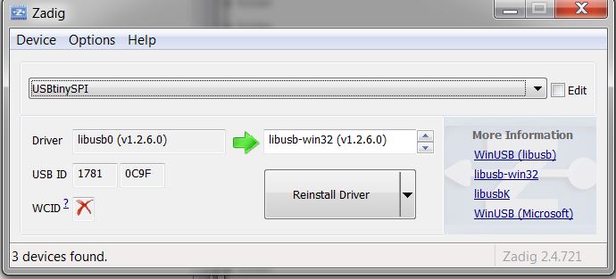
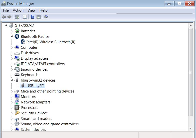
After that, I installed the driver for the programmer using Zagid.
next step was to download the source code to create HEX file. I used this source code.
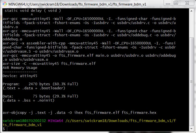
After opening the Git bash type code make to create the hex file.
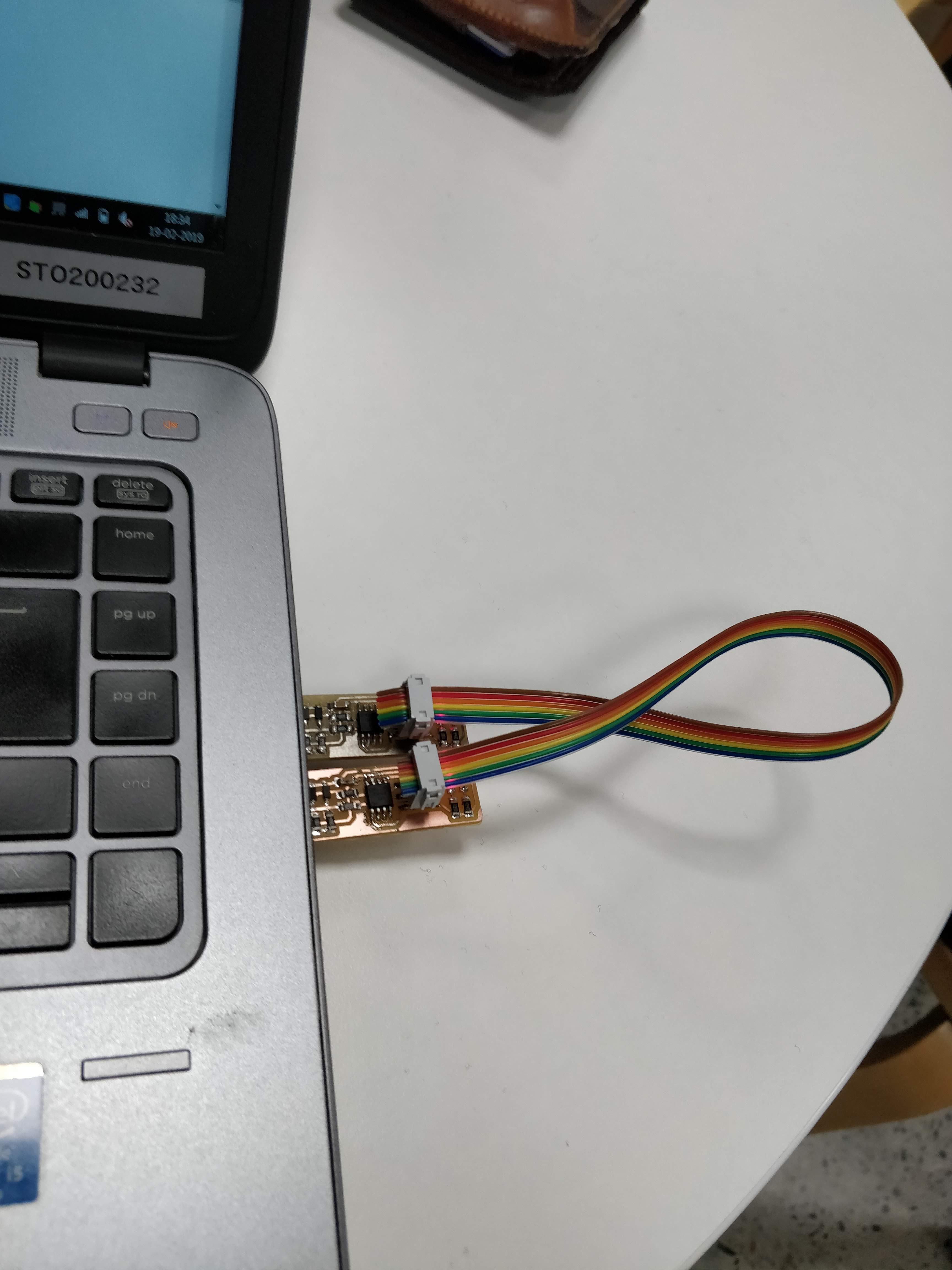
To connect the hardware and program the new system I plugged the programmer which I got from Jari ,and my board both to the computer USB port to power up. After that, we have to use the following code to make it programmable.
make flash; this will program the .hex file compiled earlier to the chip.
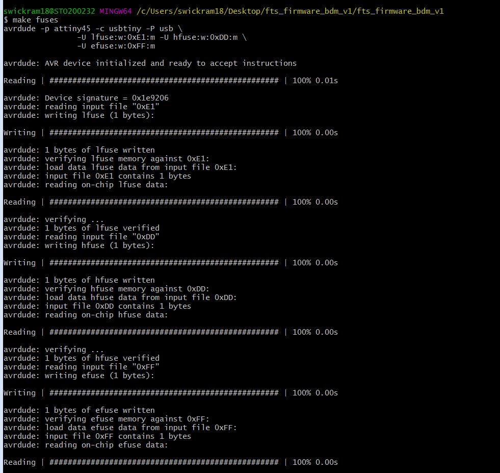
make fuses; Make the fuses except the one that makes chip not possible to program again. (Makes reset pin as normal IO-pin.)
Next we need to see whether the programmar works or not by plugging in it again.To do this unplug both programmers and plug the new one to the computers usb port, and check if it shows in windows as usb-devise.
To remove the reset ability next use command
make rstdisbl . Now the new board is ready to be used as a programmer after removing the soilder joint.
Models files
Outline for the trace
linetest trace
outline for linetrace
RML file for 0.4mm mill bit outline for Linetest
\0.4 mm flat trace & 1mm outline/linetest.interior.png.rml)
RML file for 0.4mm mill bit traces for Linetest
RML file for 0.5mm mill bit outline for Linetest
\0.5 mm flat trace & 1mm outline/linetest.interior.png.rml)
RML file for 0.5mm mill bit traces for Linetest
\0.5 mm flat trace & 1mm outline/linetest.png.rml)
HEX file for programming