Datasheet Tutorial
A lil' introduction
Datasheet are instructional manuel for electronic components. They (most of the time) explain everything concerning the component : what it does, its limitations, how to use it, etc...
Unfortunately, those documents are not written for the human eye and brain to see and understand. They were written by engineers and for engineers. Lil' moldus like us have a hard time trying to understand it ^^'
Unfortunately, those documents are not written for the human eye and brain to see and understand. They were written by engineers and for engineers. Lil' moldus like us have a hard time trying to understand it ^^'
Nevertheless, we have to try and understand it so let's see together how they are composed, and what you can learn from it :)
To try to understand how this works, best way is to dissect one together ! We'll go through the datasheet of the ATtiny24/44/84, since it's a microcontroller we use very often in Fabacademy.
This datasheet is 286 pages long. There is a summary version of 26 pages long, but it doesn't describe the microcontroller features in detail. So in order to understand properly how it works, we unfortunately have to go through the big document ^^'
I'll try to make it as understandable and complete as possible !
What is an ATtiny ?
An ATTiny is a microcontroller, which is a tiny computer designed to run small programs that can listen to or control electronic components that people connect to its “legs” (pins). It is from the AVR family.
The AVR is a modified Harvard architecture 8-bit RISC single-chip microcontroller, which was developed by Atmel in 1996.
What is the difference between the Harvard and the Von Neuman architecture ? A von Neumann architecture has only one bus which is used for both data transfers and instructions, they can not be performed at the same time. Harvard architecture has separate data and instruction busses, allowing transfers to be performed simultaneously on both busses. Microcontrollers with Harvard architecture are faster because they can read an instruction and access a data memory at the same time.
The ATTiny's program memory is flash memory. This means that when you remove power from the device, the program and data you have on it does not get erased. If your code is still uploaded in the microcontroller, it will run as soon as the ATTiny is connected to power ( battery, USB port, etc).
There are several versions of it. Here is what an ATtiny84 looks like :

What can we find in the datasheet ?
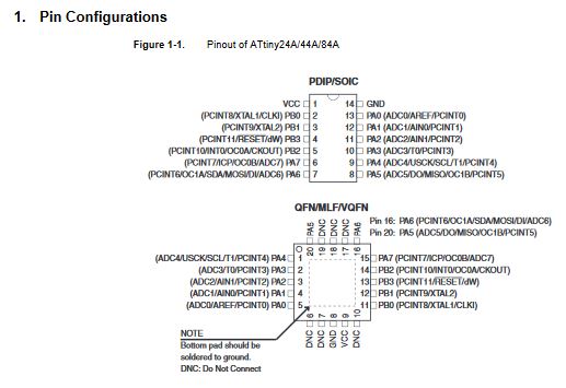
The first page is a summary of the different parts and features.
Reading these features can make us learn some stuff already. We can see from it that the ATtiny24/44/84 has high performance but is low on power.
Another interesting information : there are 3 versions of the MCU - the ATtiny24A, ATtiny44A and ATtiny84A, all with the same architecture and feature set, but with different amounts of flash memory.
We can also see that is has high endurance and non-volatile memory segments. This means that the microcontroller will last long (100 years at 25 degrees celcius and 20 years at 85 degrees celcius) and it can retain data even if there is a break in power supply. Which make it a pretty reliable microcontroller !
Stil in the temperature range features, you can see that the ATtiny can work from -40°C to +85°C. This means you can use your ATtiny for outdoor projects.
We can also see that it has ADC (analog-to-digital converter) channels. This means that the ATtiny can convert an analog signal to a digital one. We can also see that it has universal pins for serial communication. This means that we can use it for input devices, but also for output devices.
We can also see that the operating voltages for the ATtiny24/44/84 is between 1.8 and 5.5 Volts.
Pin configurations
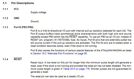
We then can find the pin configurations of the ATtiny. You can find the pinout, which are the different name of the pins on the microcontroller. Each pin has several names, because you can use the microcontroller with different systems, and each one has its own way to call out a pin.
I can see here that there are 14 pins on this chip:
- 8 x PORTA Pins : they can be inputs or outputs, and also have analog to digital converters (ADC)
- 4 x PORTB Pins : they can be programmed as inputs or outputs, and also have special functions
- Special pins on PORTB that include :
- CLKI on PB0 for external clock in
- XTAL on PB1 for manipulation of an internal oscillator
- RESET on PB3 to reset programs and perfrom timing functions
- CLKO on PB2 to output system clock data.
In the pin configurations you can also find a full description of each pin and what you can use them for.
As you can see up there, sometimes there's not much to say (like for VCC and Ground), and sometimes there's a lot to say (like for RESET or port PB3-PB0)
In there for exemple we learn that PB0-PB3 port has several internal pull-up resistors. It can be useful for some projects we make.
There are a lot of acronyms used also like : VCC (the supply voltage, commonly 5V or 3.3 V), GND for the ground, etc. These acronyms should be spelled out later in the datasheet, but if not, try Google or Wikipedia.
You can also take a look at this website where a lot of thoses acronyms are explained : http://shannonstrutz.com/component-packages.
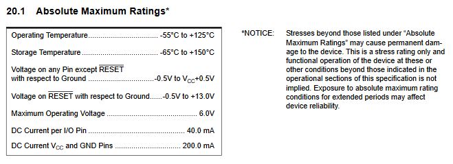
Electrical characteristics
In the "Electrical characteristics" of the datasheet, you can find a section called "Absolute Maximum Ratings". Be careful to read it carefully, coz if you ever exceed these maximum ratings you'll be possibly burning your ATtiny !
Block diagrams
You can also find what we call a block digram. It shows graphically the internal functions of the microcontroller. Usually, since it is especially focused on the inputs and the outputs of the system, it makes you have a pretty good idea on wether or not the component will be useful to your project !
Here are some tips to help you read it :
- Block diagrams use very basic geometric shapes: boxes and circles.
- The lines connecting the blocks will show you the relations between the components.
- The arrows connecting components represent the direction of signal flow through the system.
The block normally contains the name of the element or the symbol of a mathematical operation to be performed on the input to obtain the desired output.
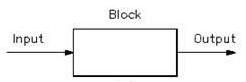
What is the difference between a block diagram and a curcuit diagram ? Unlike a block diagram or layout diagram, a circuit diagram shows the actual electrical connections. Here are some tutorials to help you read them :
Here is the block diagram of the ATtiny24/44/84 you can find in the datasheet.
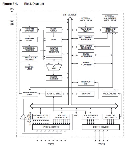
There, you can see numbers of things :
- input and output lines
- registers
- timers/counters
- PWM (pulse with modulation)
- interrupts
- ADC (analog to digital converter)
- Analog Comparator
- ...
To be completely honnest, I'm not confortable enough explaining exactly how this ATtiny block diagram up here works, but I hope the explanations I gave earlier helped you like it helped me understand more or less how to read it :)
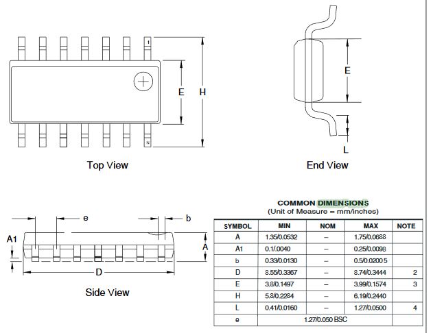
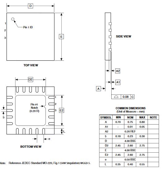
Packaging informations
You can also fin din the datasheet the packaging informations. Which means you have drawings of the microcontroller with its dimensions. Here are two exemples you can fin din the datasheet :
What is it important to learn how to read a datasheet ?
You need it to gain knowledge about the pinouts of your microcontroller. This way, you can know which pins are analog and which ones are digital.
You also need it to understand the clocks of a microcontroller. Sometimes you need to add an external one (depending on your project and on what component you are using).
Furthermore, a datasheet gives you information about the registers that are used when programming in plain C.