Eagle Tutorial
What is Eagle ?
Eagle (Easily Applicable Graphics Layout Editor) is a software that allows anyone to build electronic cards.
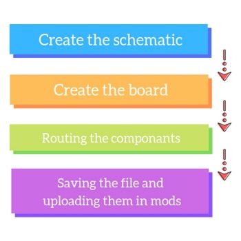
In order to build an electronic card, you need to follow different steps. Here is an illustration that summarizes it :
Step 0 : creating a new project
Eagle makes you work in “project”. Each project can have one or several schematics and boards (depending on what you need). This allows also to use a library of components and to regroup all the circuits of the same project in the same file.
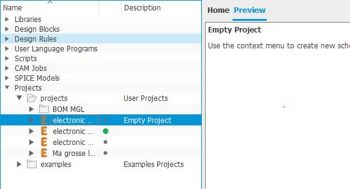
Let’s do it together so you know how to do it on your own. Once you opened Eagle, you arrive on the Control Panel.
Click on Projects > New Project
Step 1 : creating the schematic
Why do a schematic of your board ? It allows you to visualize all your components and to understand what is their use.
Easy steps to create a new one :Right click on your project name > New > Schematic
It will open a new window. It’s inside that window that we’ll draw the schematic, thanks to the library that contains all the device’s components.
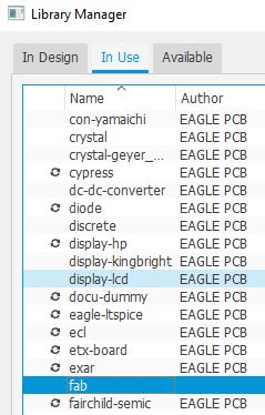
To be able to easily do your schematic, you need to download and install the Fabacademy’s components library : https://github.com/Academany/FabAcademany-Resources/blob/master/files/fab.lbr
Once you have installed it, you’ll take the schematic of your components in it. If you’ve done it right, it will appear in the library manager under the name “Fab”.
When you are looking for a component, you have to be careful with the model you’ll be using. A component is defined by two entities :
- Symbol, which is the name you’ll use when you edit a schematic
- Package, which is how the component will look like on your circuit. There are two kinds : through components and surface mounted components
For a same symbol, there can be different packages. As we are doing a SMD (Surface Mounted Device), be careful to use surface mounted components when you do yours.
How to draw your schematic ?
Add your components
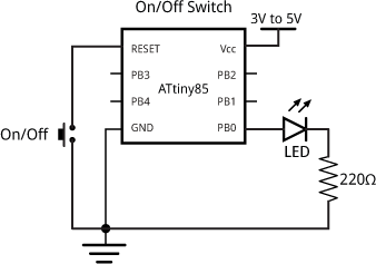
For the exemple, let’s draw a very simple schematic of a led connected to a button, throughout an ATtiny85.
If it helps, you can first hand draw it, or draw it on your computer with a simple paint software. Here is what we want to do :
On the panel on the left of your window, you click on the “Add part” button.

A window will open, from there you can access your Fab Library. Click on it to open the list, and from there you’ll choose the one you need. List them first, so you can find them more quickly.
| Name of the component | Visual |
|---|---|
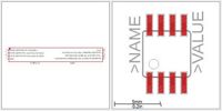
| 1 x ATTiny85 (an ATting 85 and 45 are basically the same. You won’t find an ATtiny 85 in your library, so you can use the schematic of the 45 instead) |
|
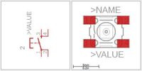
| 1 x On/Off Switch |
|
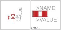
| 1 x led |
|
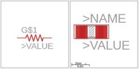
| 1 x 220 resistor |
|
Place them on your panel, I’ll show you how to connect them.
Connect the components between them
Here are some shortcuts that you will need :
- to move a component : MOVE
- to turn it : ROTATE
- to change its value : VALUE
- to change its name : NAME
- to delete something : DELETE
- to draw nets between them : NET
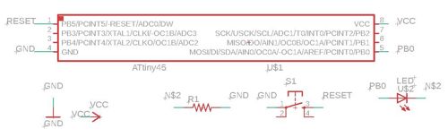
For each component, you have to connect, name and assign value to them.
Important !
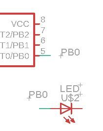
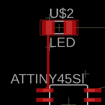
To make it easier to read, you don’t need to directly connect all the nets between them. You can draw a small one from your component and name the nets, so Eage understands they belong together. Look at the screenshot right here to understand better what I mean :
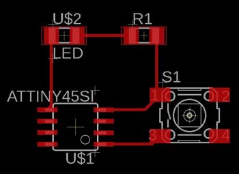
Now that you know how to do your connections, do it for all your components. You should have something like this when it’s done :
Step 2 : Create the board
In order to create your board, you have to click on the “schematic to board” button, on top of your window.
A pop-up window will open asking you if you want to create the board out of the schematic. Click OK.
A new window (Eagle loves windows) will open, with your components.
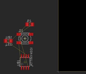
You have to place and connect them, as it will appear in your board once you milled it. Place them on the black frame of the panel.
You can see some yellow hair connecting your components. It shows you which one is connected to what. They will disappear once you have routed them. Turn them so they are the less tangled possible, otherwise it will be a difficult task to route them. Use the same command “move” to do so.
Routing the components
To route the components, write down “wire” in the search bar. Be careful to use 12mil width routes, so they are not too thin. Otherwise the milling will be complicated.
Here is what it should look like once the route is drawn :
Here is the result when they all are connected (see, all the yellow hairs are gone!) :
Checking your work
Now that everything is ready, a little last thing to be sure everything is perfect. Use the DRC tool, that will detect any problem or error.
To do so, write in the search bar “DRC” and a new window will open.
You can change those parameters, so if there’s a problem (two routes that touches each other, misplaced routes, etc) it will appear automatically.
Step 3 : Drawing the outlines
Now that we have all our components set up, we have to draw the outlines !
Click on “polygon”, and from there you select “milling” in the layer list. You just have to draw the outlines around your board and it’s done ! This is what it should look like (depending on what your draw, I kept it simple) :)
Step 4 : Export your work in PNG
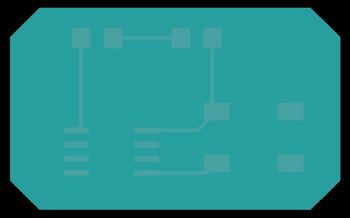
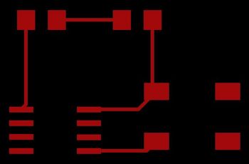
First, you need to choose the layer you want to export in PNG. We want the traces and the outlines. You have to go to the layer settings, and a window will open. There, you can click on “hide layers” and select only the layer “top” to begin.
And this will appear this way :
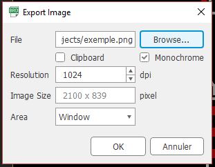
After that, you should do : File > Export > Image
A pop-up window will open. There, select “monochrome”, a resolution of 1024 dpi, and select “window”. And choose where you want to save your file !
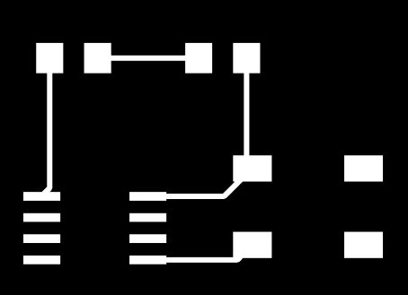
This is the PNG file you should obtain :)
Same process for the outline, you should select “milling” in the layers and then export it.

You are all set to mill your PCB ! :)
Wanna go further ?
Here are some tutorials :
| Name of the website | Link |
|---|---|
| Using EAGLE: Schematic | https://learn.sparkfun.com/tutorials/using-eagle-schematic/all#wiring-up-the-schematic |
| PCB Design using EAGLE – Part 1: Introduction to EAGLE and Software Environment | http://maxembedded.com/2014/06/pcb-design-eagle-part-1-introduction-eagle-software-environment/ |
| Introduction to Eagle | http://fabacademy.org/2018/docs/FabAcademy-Tutorials/week6_electronic_design/eagle_english.html |