7. Electronics design
Group assignment
Use the test equipment in your lab to observe the operation of a microcontroller circuit board
Individual assignment
Redraw one of the echo hello-world boards or something equivalent, add (at least) a button and LED (with current-limiting resistor) or equivalent input and output, check the design rules, make it, test it.
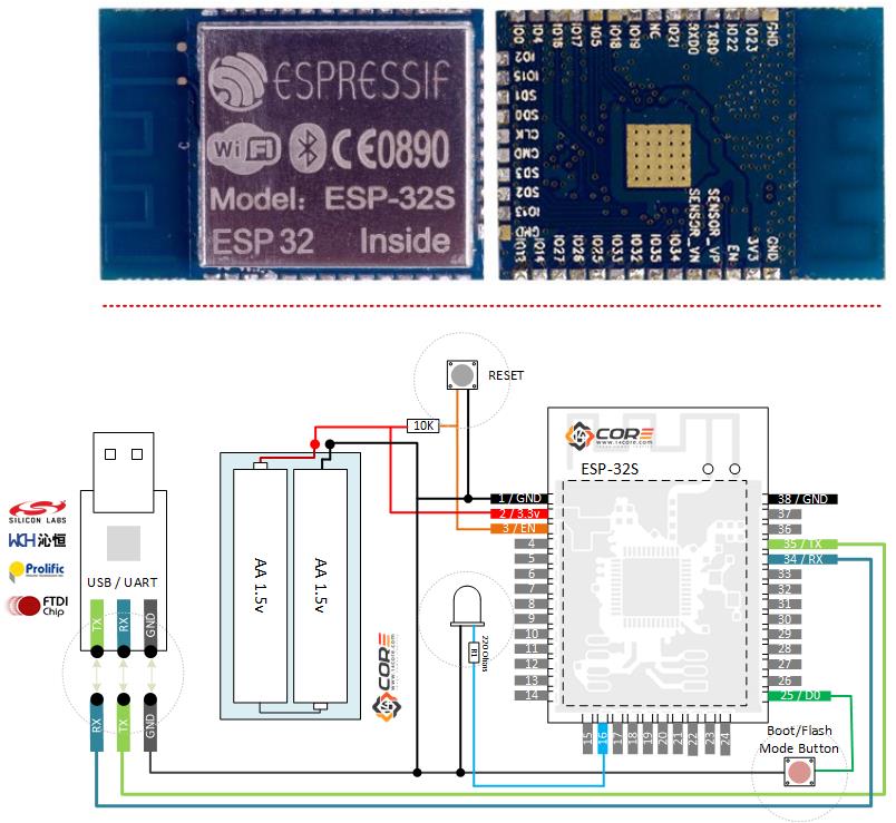
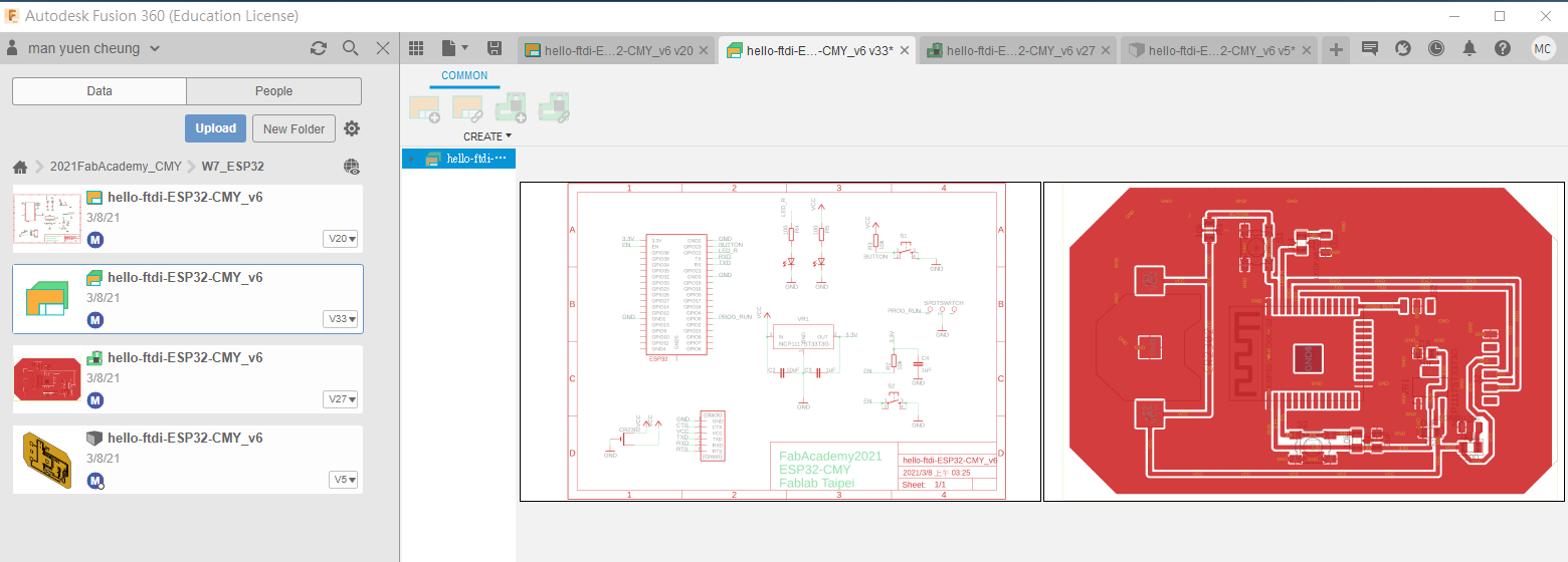
I want to use the ESP32 to do my individual assignment.Before I have some experience using Frizing. It is my first to use fusin360 to design the schematic and PCB. It is challenge and funny week for me.
Summary
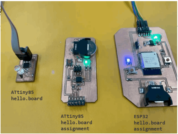
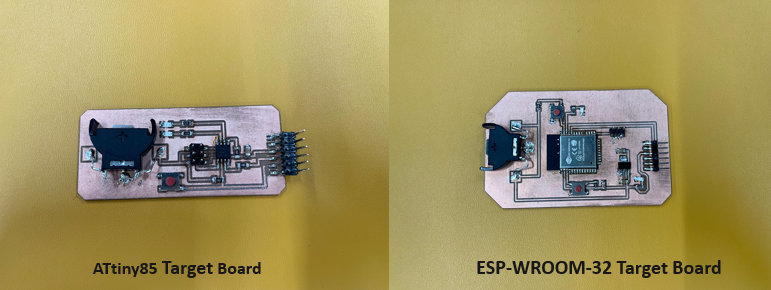
Before starting ESP32.hello.ftdi board, I build a ATtiny85.hello.ftdi first. I try add two LEDs, one button and CR-2303 battery holder to modify the ATtiny85.hello.board. It let me more soldering practice and familiar using fusion360 PCB Design when designing the PCB. Keep in mind placing components in the right orientation and debug the circuit when soldering each component to prevent short or cold joint.
Learning Outcomes
Theory and use of things i learnt from this assignment:
-
Select and use software for circuit board design.
-
Demonstrate workflows used in circuit board design.
Useful links and my individual assignment download
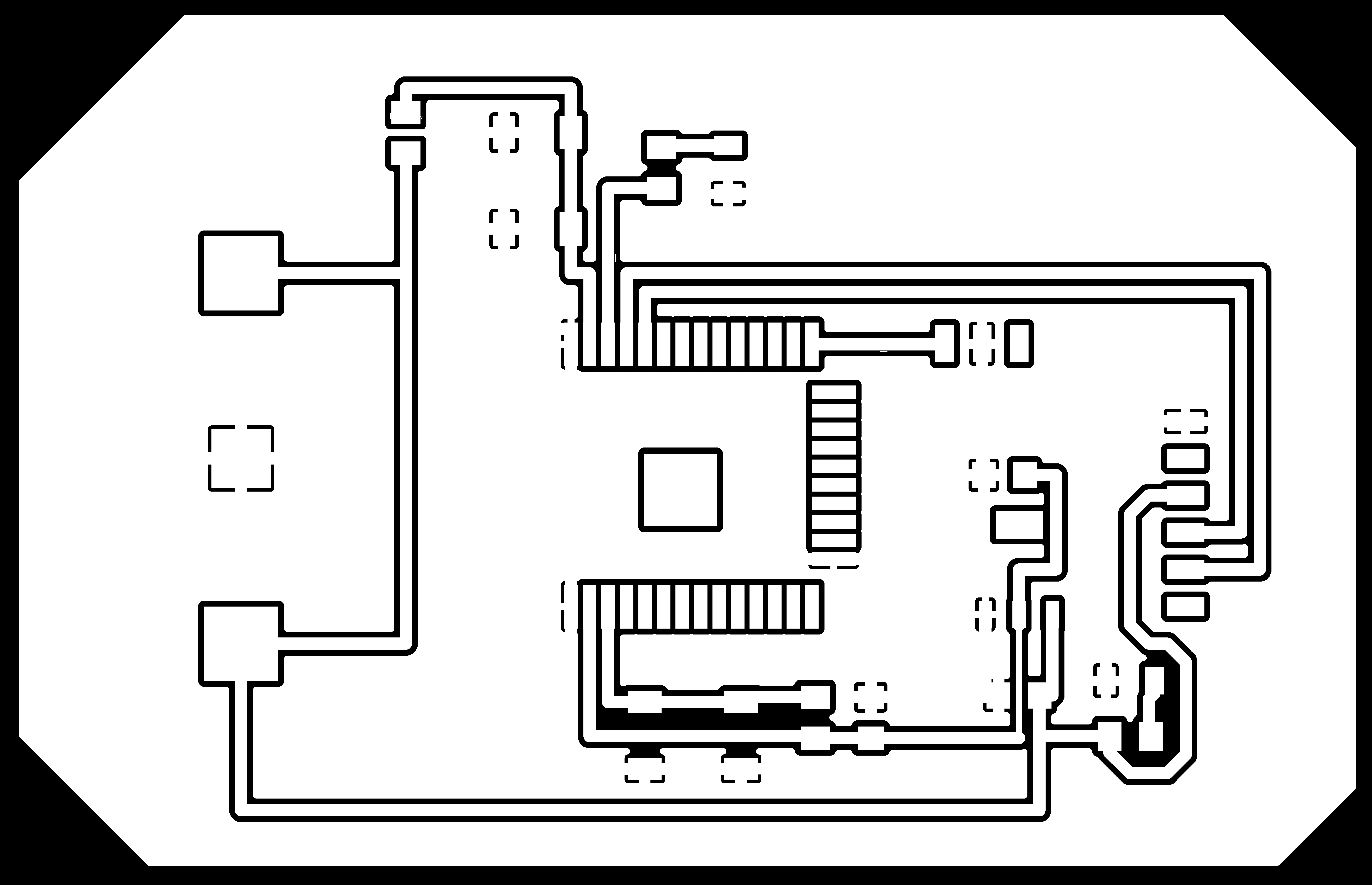
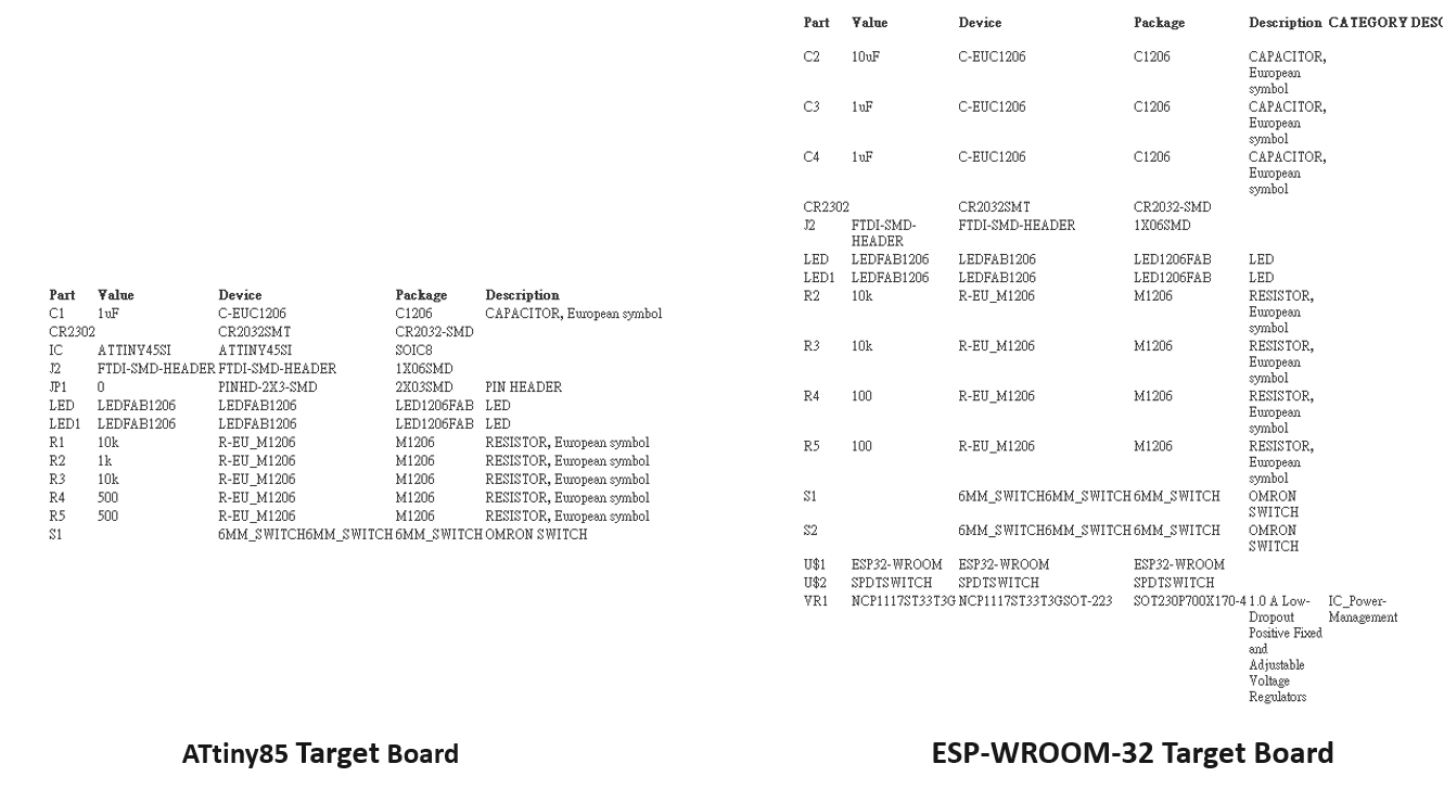
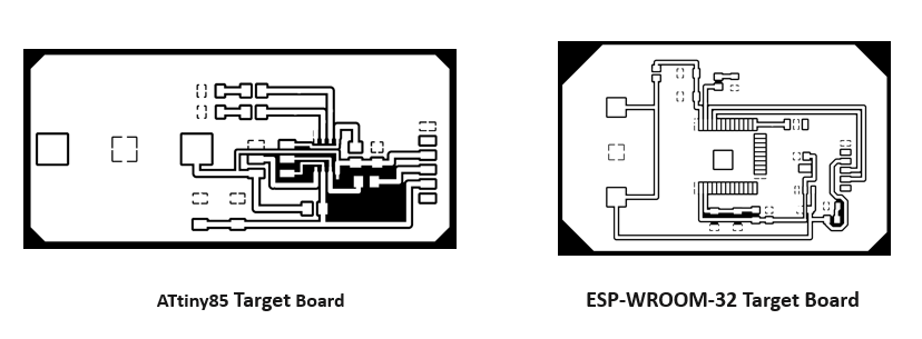
ATtiny45 board components traces interior
pin re-use echo.serial.ino video
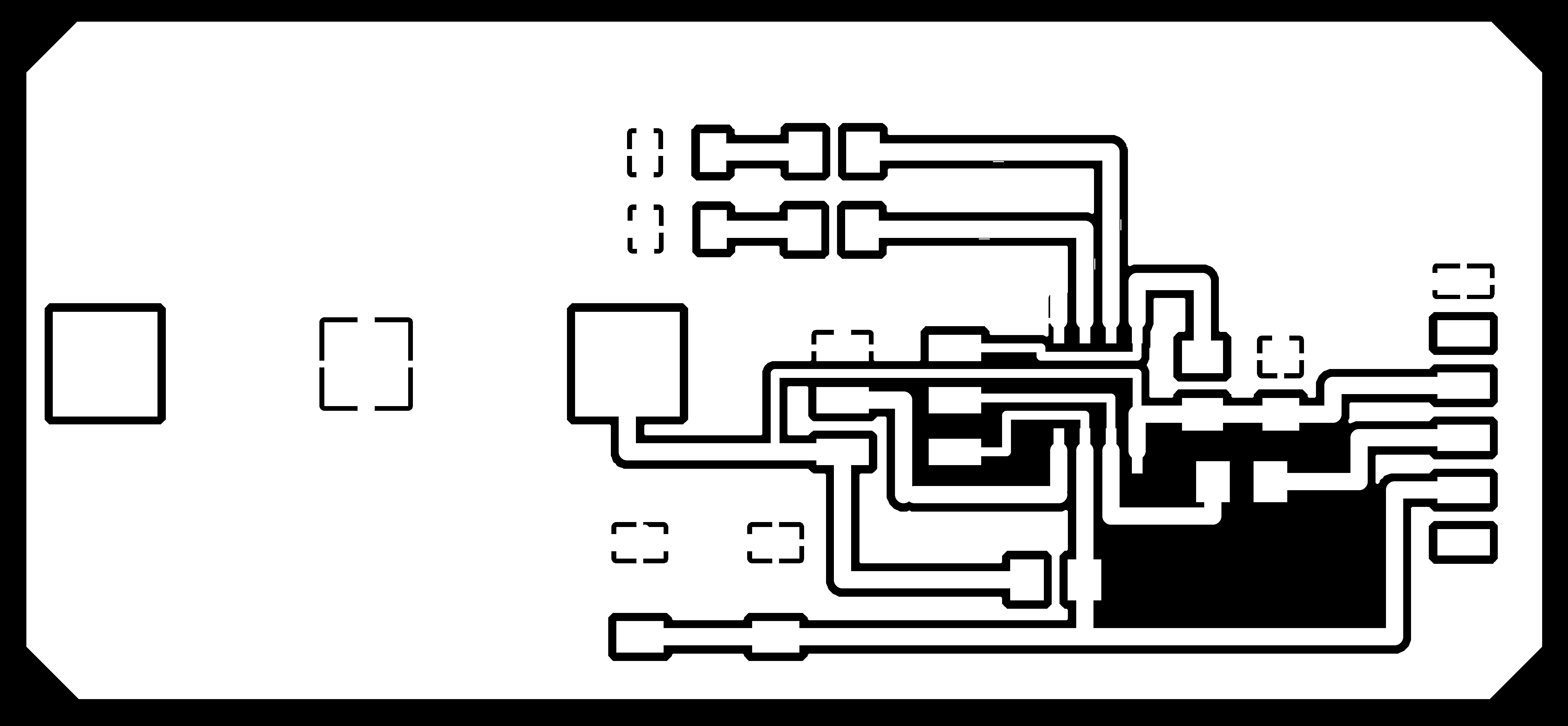
ESP-WROOM-32 board components traces interior
pin re-use echo.serial.ino video
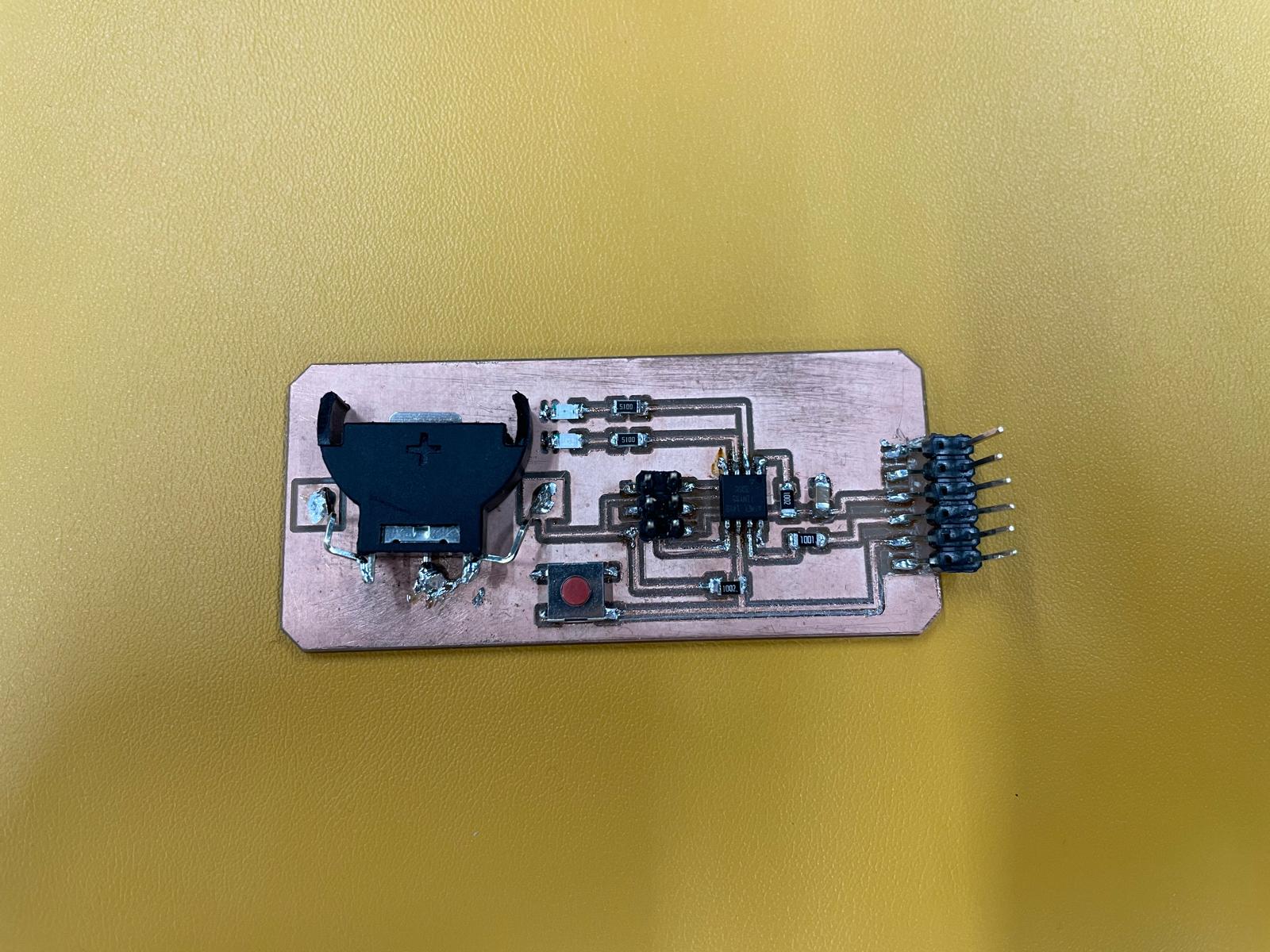
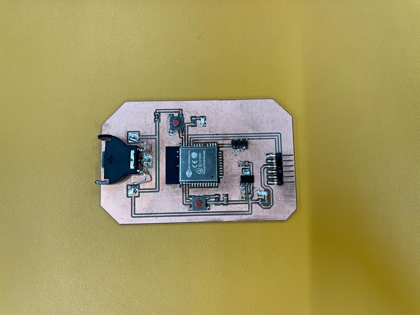
Milling & Soldering
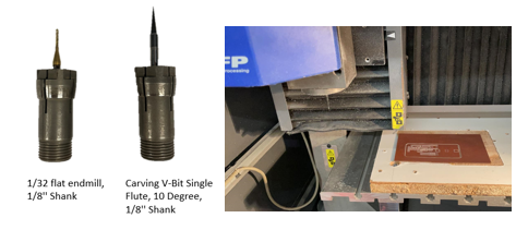
In the Fablab laboratory, we all choose Roland-MDX500 for machine milling. Although it is not suitable for mass production, it is convenient for rapid prototyping and is more environmentally friendly. The machine used for marking is a milling machine, a 10 degree Carving V-bit is used to engrave the circuit trace, and a 1/32 flat endmill is used to cut out the outer edge of the entire board.
PCB Design Rules
| Setting | DESCRIPTION |
|---|---|
| Clearance | 0.42mm |
| Track Width | 1mm |
| Sizes | 0.4mm |
I decide make a single PCB for milling.
Work Flow
- Design your circuit.
- Make schematic diagram of components used in your circuit.
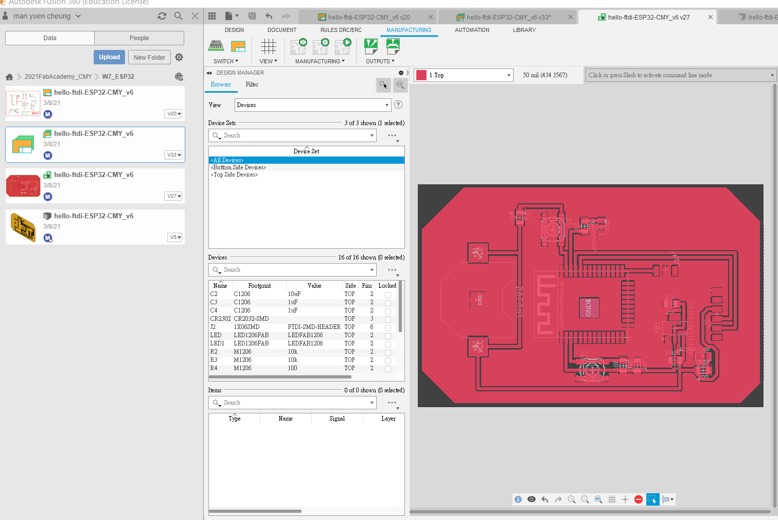
- Transfer schematic diagram to PCB editor and route tracks.
- Mill board.
- Solder board.
- Test board.
Design your circuit.
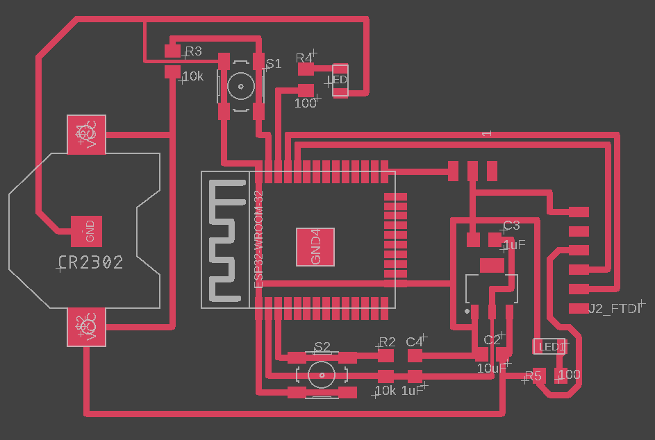
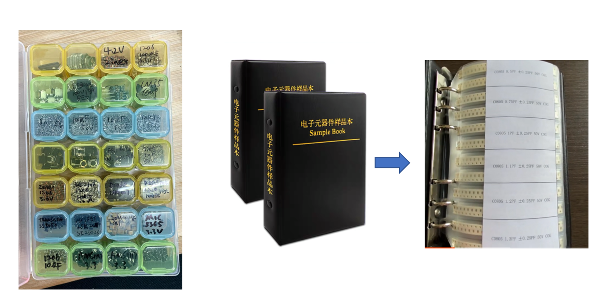
During this week, I work with ATtiny85 and ESP32. Redraw and Customize a board with Fusion360. I keep all electronic parts with IC stamp book and nano-box buy from Taobao.
I have some experiments with fusion360. Fusion 360 Integration with EAGLE,it can streamline your electrical and mechanical design workflows together. I then tried to redraw and customize a board for my assignment.
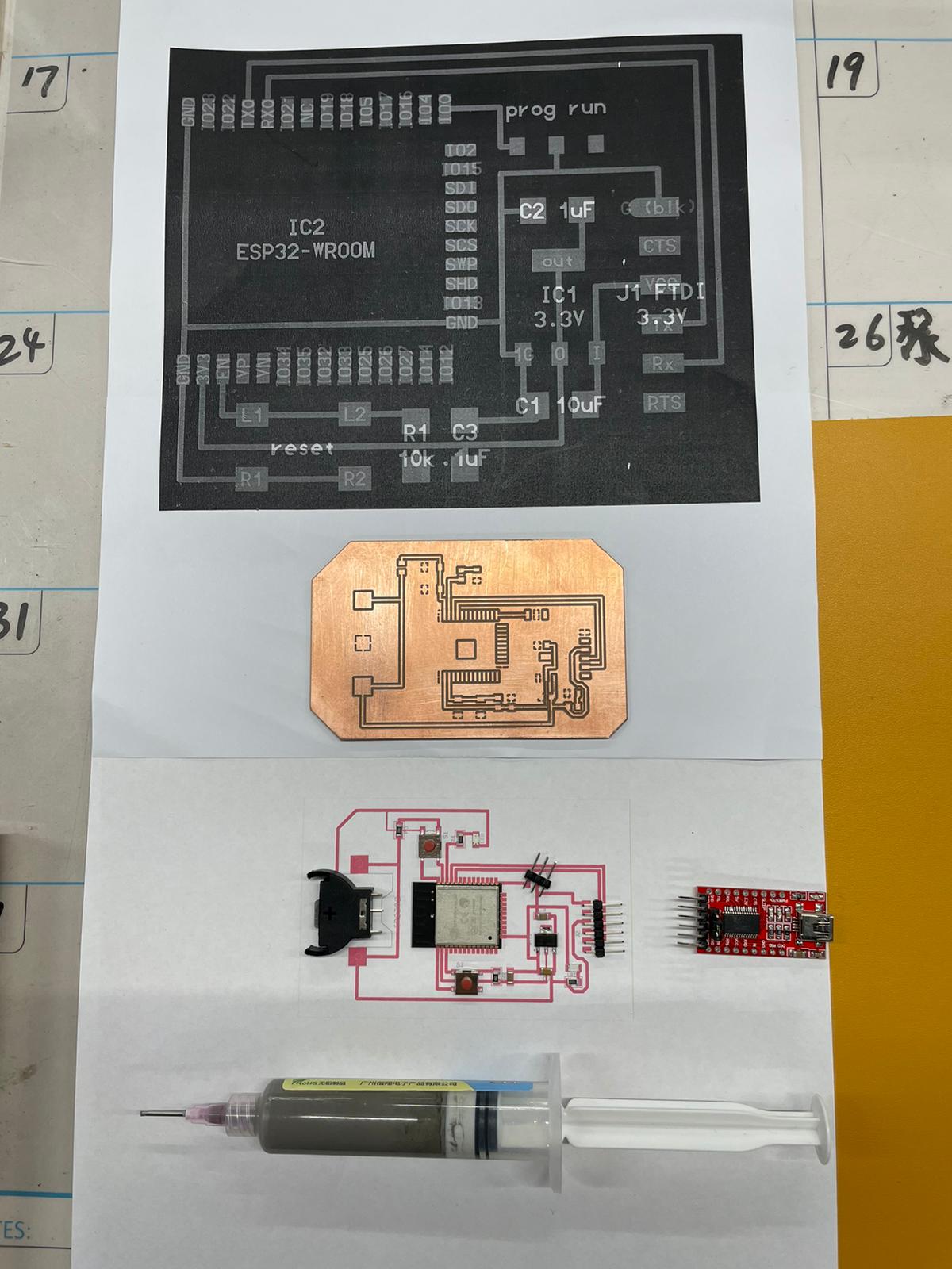
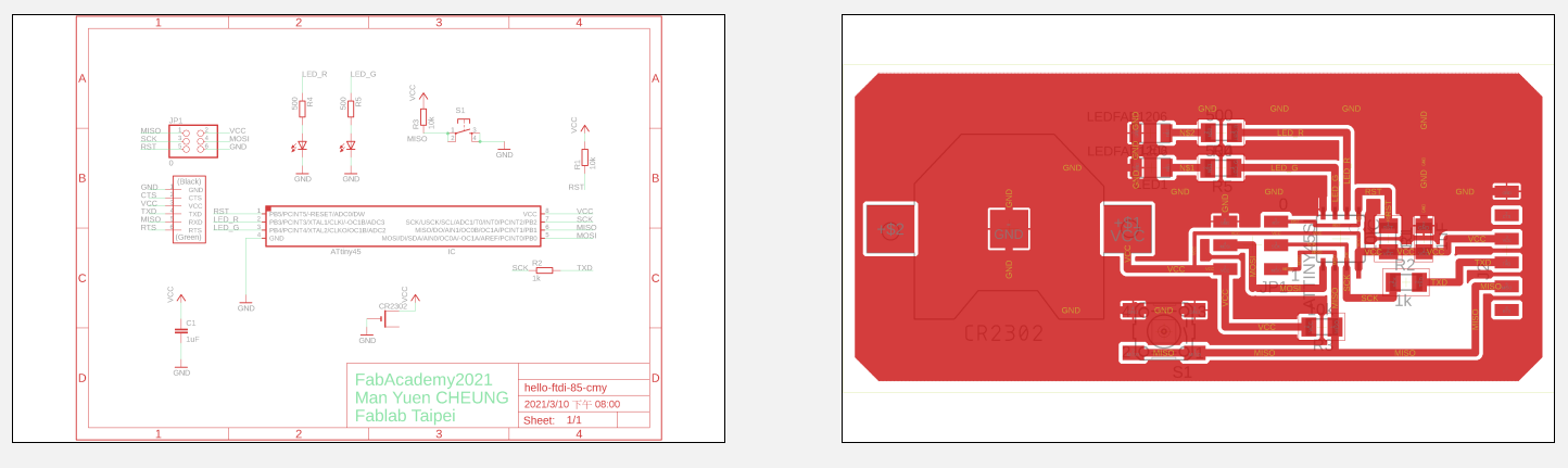
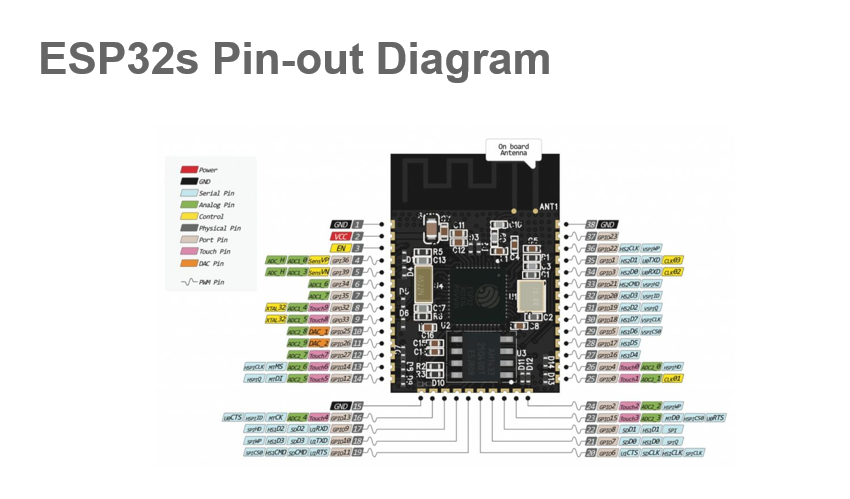
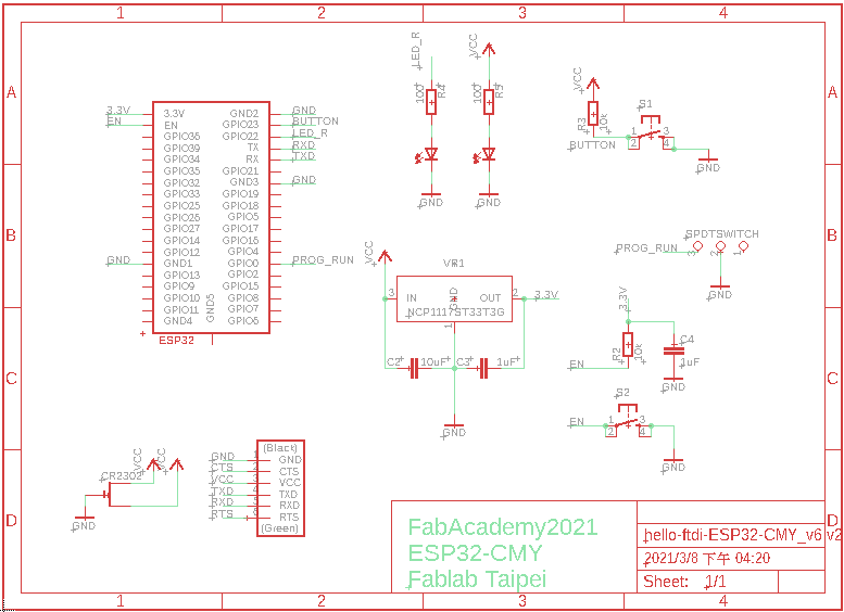
I decided to add a LED and a switch to a hello.ESP32-WROOM board. To meet course requirements I re-drew the entire schematic and added my switch and led. I used Fusion360 Electronic Design to accomplish this task. Here are the steps I took:
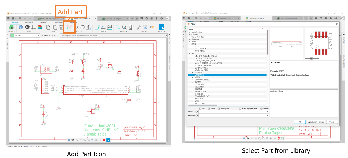
Using the [ADD PART] button i added the components from the Fablab library to the diagram. It doesn’t matter really when the components are placed on the diagram, as the purpose of the schematic diagram is to make connections and relationships between the components.
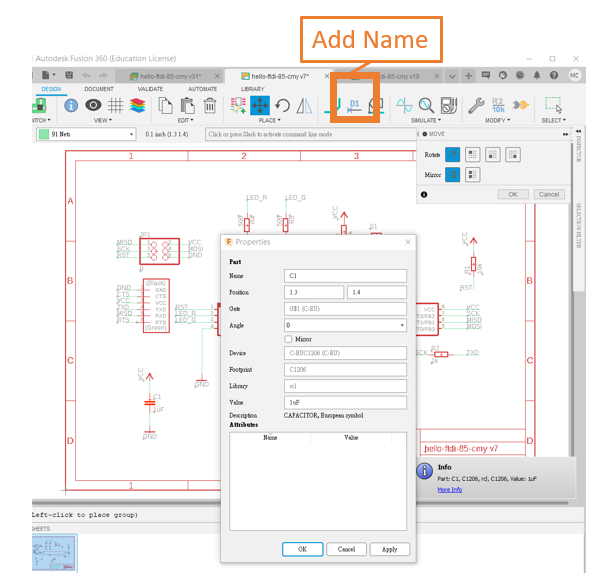
Adding [ NAME ] to the various legs of the components allowed the software to know where and how the different components need to be attached. For human reference, i annotated the symbols using the [ Properties ] and labelled the values of each component from the Properties dialogue box.
If needed, check with the component manufacturer’s website / data sheets on their function and how to map the different pins etc.
Make Schematic Diagram:
Tips:
Rotate the components for easier routes. If the component is big enough, you maybe able to run a track underneath it and through its pads. Sometimes tracks may have to go around an obstacle and attach from ‘behind’.
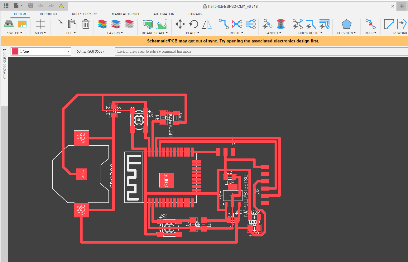
Mill board.
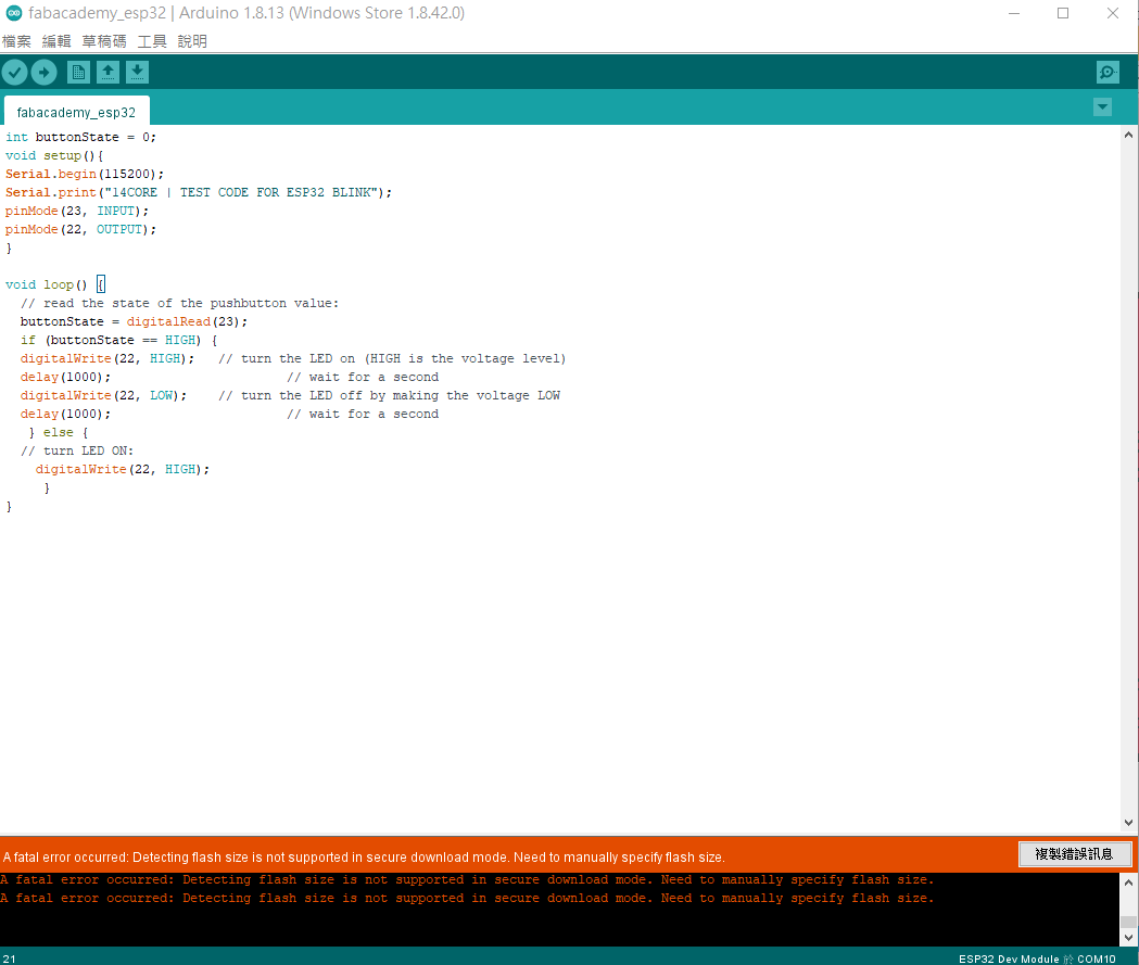
Here the problems started, entirely with issues coming from exporting .SVG from Fusion360 PCB Design and importing into Fab modules. I cannot export image from Fusion360. Finally, I use Eagle CAD to solute the problem.
Solder board.
Lessons to take away
Design PCB boards to match your expertise in soldering. Don’t position components on a board closer together than your CNC can milling and you can solder. Routing PCB should follow the design rule. New exprience for me using LEAD-FREE Solder Paste to stuff SMT IC.
ATtiny85 Code Example Prepare
int buttonState = 0;
// the setup function runs once when you press reset or power the board
void setup() {
  // initialize digital pin LED_BUILTIN as an output.
  pinMode(1, INPUT);
  pinMode(3, OUTPUT);
  pinMode(4, OUTPUT);

}

// the loop function runs over and over again forever
void loop() {
  // read the state of the pushbutton value:
  buttonState = digitalRead(1);
  if (buttonState == HIGH) {
  digitalWrite(3, HIGH);   // turn the LED on (HIGH is the voltage level)
  digitalWrite(4, LOW);   // turn the LED on (HIGH is the voltage level)
  delay(500);                       // wait for a second
  digitalWrite(3, LOW);    // turn the LED off by making the voltage LOW
  digitalWrite(4, HIGH);   // turn the LED on (HIGH is the voltage level)
  delay(500);                       // wait for a second
   } else {
  // turn LED off:
    digitalWrite(3, HIGH);
    digitalWrite(4, HIGH);
     }
ESP32 Code Example Prepare
int buttonState = 0;
void setup(){
Serial.begin(115200);
Serial.print("14CORE | TEST CODE FOR ESP32 BLINK");
pinMode(23, INPUT);
pinMode(22, OUTPUT);
}

void loop() {
  // read the state of the pushbutton value:
  buttonState = digitalRead(23);
  if (buttonState == HIGH) {
  digitalWrite(22, HIGH);   // turn the LED on (HIGH is the voltage level)
  delay(1000);                       // wait for a second
  digitalWrite(22, LOW);    // turn the LED off by making the voltage LOW
  delay(1000);                       // wait for a second
   } else {
  // turn LED ON:
    digitalWrite(22, HIGH);
     }
Forget to collect the Boot/Flash Mode Jumper