Input Devices Assignment 11
Assignment 11
As I am going to do a Mouse in Final Project .. So I started thinking about how it will looks like my input circuit ..
I am going to need a Analog joystic to can read the directions and have pushbutton to use a click for the mouse as a Left click
I need also a Bluetooth to make it can use it wirelessly ..
I need FTDI and ISP to can Program and test it serially before applying Bluetooth in the Communication Assignment ..
So It will consists of these :
BOM :
Main Board As a Block
1) Attiny 44
2) Res 10k
3) Cap 10UF
4) ISP Connector
5) FTDI Connector
Then I Added my special Circuit Component :
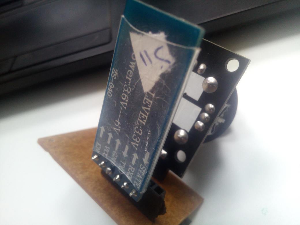
1) Bluetooth Pin Header
2) Joystic Pin Header
3) Analog Joystic Module
4) Bluetooth HC-05
For Joystic You need to take in consideration the Orientations of the Pins and Its arrngement ..
also Take in Consideration the arrange of the Pins of the Bluetooth to can deliver power and read data right .. and take care of the Orientation you will use ..
You can Find here all component I used with links where to buy it and it is name to can find datasheet ..
Component | Amount | Price for 1 | Link |
Res 10K | 2 | $0.05 | |
Res 499 | 4 | $0.05 | |
Capacitor 10UF | 2 | $0.1 | |
RED LEDs | 4 | $0.25 | |
FTDI Header | 1 | $0.25 | |
HC-05 Bluetooth Module | 2 | $17 | |
ATTINY44A-SSU-ND | 2 | £0.596 | |
ISP Pin Header | 2 | $0.83 | |
Female Pin Header | 17 Pin | $0.1 | |
Analog Joystic | 1 | $2 |
https://store.fut-electronics.com/products/joystick-module-4-directions This is my plan for this task :
1) Design
2) Fabricate
3) Soldering
4) Coding
5) Testing
Task 1
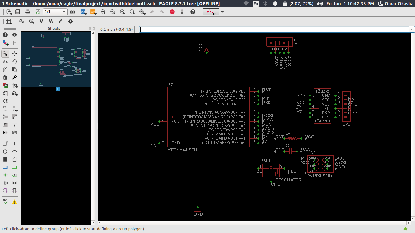
I start Designing .. For Designing I followed the same Steps in Electronics Design Week
But as I go before this a lot of issues with Fabricating PCBs ..
So I made a lot of design and I get bored from making the Main Board alot in the designs
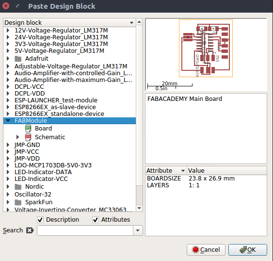
So I found Something called Design Blocks ..
And I was really Facinated ..
That I can Draw a Schematic and Board for one Time and Make Save as a design Block ..
Then you will Find it in you Design blocks .. Which makes it super easy ..
Then I start Building on it .. and this is the result ..
Task 2
For Fabricationg I followed the same Steps in Electronics Production Week
Here are the Files to Be fabricated on CNC ..
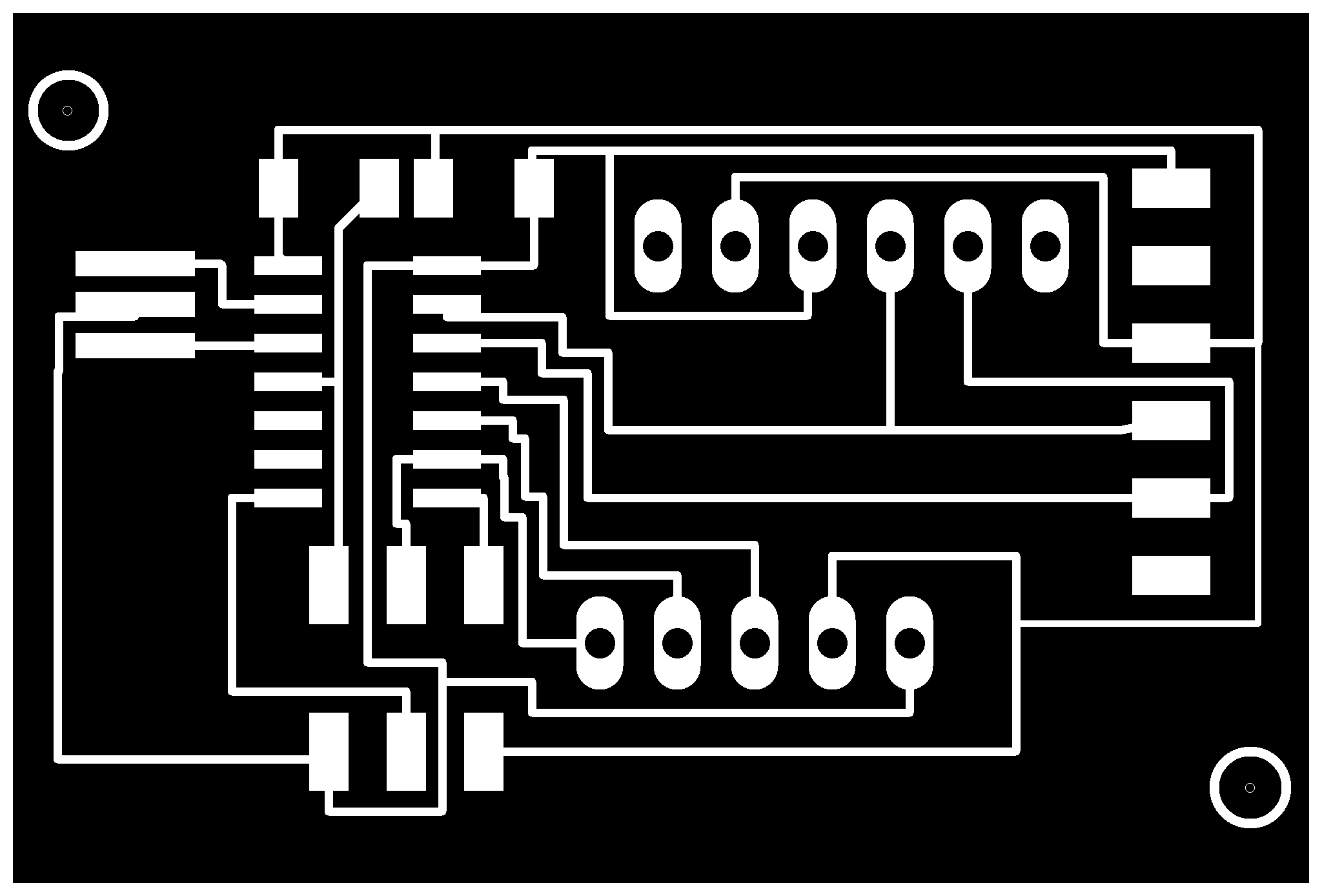
Then I start to To fabricate it ..
Task 3
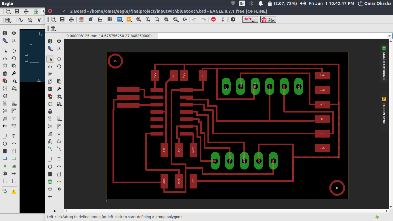
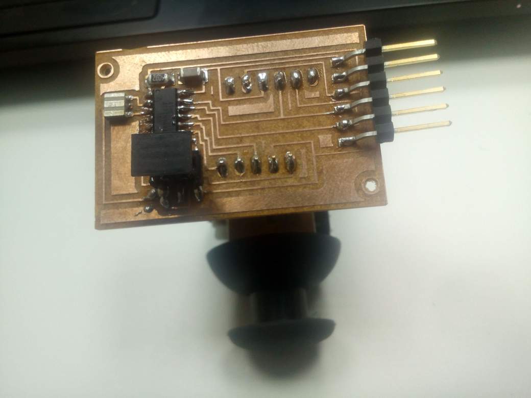
Then This is How it looks like my Final Input PCB ..
This how it looks like with Component
Task 4
This is the code I am Going to Use ..
This code Read 3 Things Read the Analog Data from x and y .. and Read Digital Data for the Push Button and Send it Over Serial To the PC to Test the Circuit working ..
Important Note about the code : I Divided the Values of Analog on 100 To can reduce the Noise ..
To Understand the Code Syntax and How I Wrote it .. You can Check my Embedded programming Assignment As I made There a full Illustrating for How to use Arduino and What is all Functions I used There ..
     #include‹SoftwareSerial.h›


#define BUTTON PA3
#define x PA2
#define y PA3
#define btn PA4

#define val 0

#define tx PA0
#define rx PA1
SoftwareSerial ser(rx, tx);
void setup() {
  // put your setup code here, to run once:

ser.begin(9600);
}

void loop() {
  // put your main code here, to run repeatedly:
ser.print("Switch:  ");
  ser.print(digitalRead(btn));
  ser.print("\n");
  ser.print("X-axis: ");
  ser.print(analogRead(x))/100;
  ser.print("\n");
  ser.print("Y-axis: ");
  ser.println(analogRead(y)/100);
  ser.print("\n\n");
  delay(500);
}
Task 5
This is it :D :D The Working Circuit