7. Electronics design
concepts and KiCAD
Aims
Since I do not have any idea about electronic design this week was a bit challenging for me. I had an experience with the arduino uno and nano but I tried to go deeper into this scope.
So for this week assignment I was trying to design a board that I will need for my final project. This board should be able to control a stepper motor which I need it for moving food in my vending machine. I also thought about camera module or wi-fi communicator. But I think I will leave them for further development of my control center of the vending machine.
Group assignment
For this group assignment I measured the current and voltage on Barduino board.
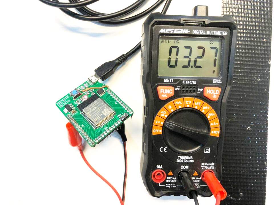
Fig01- measuring the 3V3 from Barduino
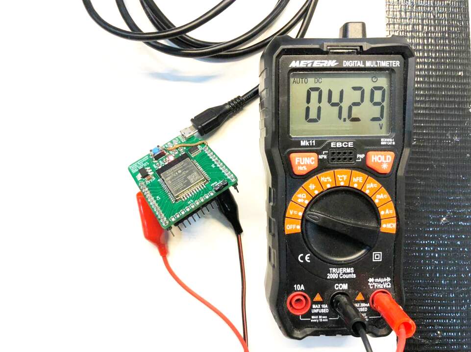
Fig02- measuring the 5V from Barduino
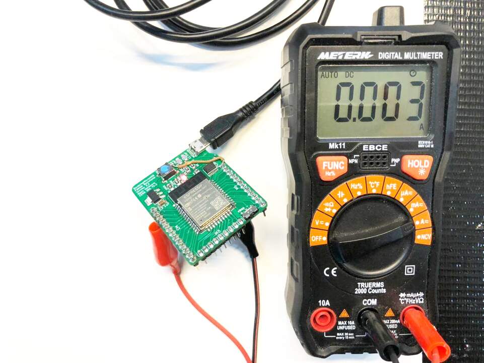
Fig03- measuring the current from the Barduino pin
By this assignment I learned how to use a multimeter and measure voltage, and current. Also I learned how to make continuity check on the circuit to debug the board.
Principle
voltage current resistor
based on Bohr
voltage (V) :
difference of the charge between to cathodes.
Current (I) : Amp
resistor (R) : how easy the current passed through the material.
conventional direction of the
hums low: V= I*R p= I^2R
Energy sources: From form to form
resistor: Calculation code colors
capacitors (F): store Energy filter the noise
diode: control the current flow direction limit voltage that diode can eliminate to pass
Zener clipping the voltage
Oscillator/Resonators(Hz):
transistor:
combination and sequential pub/electronics/lib
PCB design Processes
Before jump into the tools and resources I want to share an overall vision of the journey. To start the board design first we need to have clear idea about the purpose of the PCB. They can have multiple or single tasks but it should be clear. Base on those tasks you will piking components which they may be are in the inventory of the lab or available online. Then we need to go through the datasheets of those component and check their power dependencies. Sometimes they include some schematic of how they should be used. Note that it is the best always to check the datasheets from the manufacturer instead of blogs/stock flows many component are available from different manufacturer and going through those resources sometimes will be a bit confusing. After study of each component and their usage, we need to make a schematic of the circuit. This can be done in the software and digital form which will facilitate the process. The software is going to generate a text base file with certain protocols.
This is a definition of the component in .sch files
$Comp
L fab2020:A4953-H-BRIDGE-MOTOR-DRIVER M1
U 1 1 5E64F1CF
P 9250 3500
F 0 "M1" H 9250 3500 45  0001 C CNN
F 1 "A4953-H-BRIDGE-MOTOR-DRIVER" H 9250 3500 45  0001 C CNN
F 2 "fab-SOIC8" H 9280 3650 20  0001 C CNN
F 3 "" H 9250 3500 50  0001 C CNN
    1    9250 3500
    1    0    0    -1
$EndComp
definition of the connections in the .sch files
Wire Wire Line
    3250 1150 3250 1400
Wire Wire Line
    3250 1400 3650 1400
Wire Wire Line
    3750 950  3650 950
Wire Wire Line
    3650 1100 3650 950
Connection ~ 3650 950
Wire Wire Line
    3650 950  3550 950
Wire Wire Line
    2600 950  2750 950
Wire Wire Line
    5550 3550 5400 3550
Wire Wire Line
    5500 4050 5400 4050
Wire Wire Line
    5500 4150 5400 4150
Wire Wire Line
    5500 4250 5400 4250
Wire Wire Line
    5500 4350 5400 4350
After making .sch file base on the footprint libraries and connections it will generate a .net file. This file is like a json file but with totally different syntax.
component tages
(components
    (comp (ref C3)
      (value 10uf)
      (footprint fab-C1206)
      (libsource (lib fab2020) (part CAP-UNPOLARIZED) (description ""))
      (sheetpath (names /) (tstamps /))
      (tstamp 5E642A9B))
    (comp (ref C5)
      (value 10uf)
      (footprint fab-C1206)
      (libsource (lib fab2020) (part CAP-UNPOLARIZED) (description ""))
      (sheetpath (names /) (tstamps /))
      (tstamp 5E64340A))
    (comp (ref C1)
      (value 0.1uf)
      (footprint fab-C1206)
      (libsource (lib fab2020) (part CAP-UNPOLARIZED) (description ""))
      (sheetpath (names /) (tstamps /))
      (tstamp 5E643949))
    (comp (ref C4)
      (value 0.1uf)
      (footprint fab-C1206)
      (libsource (lib fab2020) (part CAP-UNPOLARIZED) (description ""))
      (sheetpath (names /) (tstamps /))
      (tstamp 5E6445F7))
    (comp (ref C6)
      (value 0.1uf)
      (footprint fab-C1206)
      (libsource (lib fab2020) (part CAP-UNPOLARIZED) (description ""))
      (sheetpath (names /) (tstamps /))
      (tstamp 5E644B89))
footprint library
(libparts
  (libpart (lib PJ1-023-SMT-TR-FABJack) (part PJ1-023-SMT-TR)
    (fields
      (field (name Reference) J)
      (field (name Value) PJ1-023-SMT-TR)
      (field (name Footprint) CUI_PJ1-023-SMT-TR)
      (field (name Datasheet) "CUI INC")
      (field (name Field4) "Manufacturer recommendations")
      (field (name Field5) 1.05))
    (pins
      (pin (num 1) (name 1) (type passive))
      (pin (num 2) (name 2) (type passive))
      (pin (num 3) (name 3) (type passive))
      (pin (num 4A) (name SHIELD) (type passive))
      (pin (num 4B) (name SHIELD) (type passive))))
  (libpart (lib fab2020) (part A4953-H-BRIDGE-MOTOR-DRIVER)
    (footprints
      (fp *SOIC8*))
    (fields
      (field (name Reference) M)
      (field (name Value) A4953-H-BRIDGE-MOTOR-DRIVER)
      (field (name Footprint) fab-SOIC8))
    (pins
      (pin (num 1) (name GND) (type BiDi))
      (pin (num 2) (name IN2) (type BiDi))
      (pin (num 3) (name IN1) (type BiDi))
      (pin (num 4) (name VREF) (type BiDi))
      (pin (num 5) (name VBB) (type BiDi))
      (pin (num 6) (name OUT1) (type BiDi))
      (pin (num 7) (name LSS) (type BiDi))
      (pin (num 8) (name OUT2) (type BiDi))))
nets tag which is defining which pins are connected together
(nets
    (net (code 1) (name "Net-(IC1-Pad10)")
      (node (ref M1) (pin 3))
      (node (ref IC1) (pin 10)))
    (net (code 2) (name V12)
      (node (ref M1) (pin 5))
      (node (ref M2) (pin 5))
      (node (ref J1) (pin 1))
      (node (ref C5) (pin 2))
      (node (ref C3) (pin 1))
      (node (ref C2) (pin 1))
      (node (ref IC2) (pin 2))
      (node (ref C6) (pin 2))
      (node (ref C4) (pin 1)))
    (net (code 3) (name "Net-(IC1-Pad13)")
      (node (ref M2) (pin 2))
      (node (ref IC1) (pin 13)))
Based on the data in the .net file pcb software tools will make file with the graphical footprints and net connection between the components. In this interface, we position the footprints and trying to design a trace to connect the nets together without interfering with each other.
component footprint representation in the KiCAD_pcb file
(module fab-C1206 (layer F.Cu) (tedit 200000) (tstamp 5E81311F)
    (at 110.236 77.724)
    (descr CAPACITOR)
    (tags CAPACITOR)
    (path /5E643949)
    (attr smd)
    (fp_text reference C1 (at 1.905 -1.905) (layer F.SilkS)
      (effects (font (size 1.27 1.27) (thickness 0.1016)))
    )
    (fp_text value 0.1uf (at 2.54 1.905) (layer F.SilkS)
      (effects (font (size 1.27 1.27) (thickness 0.1016)))
    )
    (fp_line (start -1.7018 0.8509) (end -0.94996 0.8509) (layer F.SilkS) (width 0.06604))
    (fp_line (start -0.94996 0.8509) (end -0.94996 -0.84836) (layer F.SilkS) (width 0.06604))
    (fp_line (start -1.7018 -0.84836) (end -0.94996 -0.84836) (layer F.SilkS) (width 0.06604))
    (fp_line (start -1.7018 0.8509) (end -1.7018 -0.84836) (layer F.SilkS) (width 0.06604))
    (fp_line (start 0.94996 0.84836) (end 1.7018 0.84836) (layer F.SilkS) (width 0.06604))
    (fp_line (start 1.7018 0.84836) (end 1.7018 -0.8509) (layer F.SilkS) (width 0.06604))
    (fp_line (start 0.94996 -0.8509) (end 1.7018 -0.8509) (layer F.SilkS) (width 0.06604))
    (fp_line (start 0.94996 0.84836) (end 0.94996 -0.8509) (layer F.SilkS) (width 0.06604))
    (fp_line (start -0.19812 0.39878) (end 0.19812 0.39878) (layer F.SilkS) (width 0.06604))
    (fp_line (start 0.19812 0.39878) (end 0.19812 -0.39878) (layer F.SilkS) (width 0.06604))
    (fp_line (start -0.19812 -0.39878) (end 0.19812 -0.39878) (layer F.SilkS) (width 0.06604))
    (fp_line (start -0.19812 0.39878) (end -0.19812 -0.39878) (layer F.SilkS) (width 0.06604))
    (fp_line (start -2.47142 -0.98298) (end 2.47142 -0.98298) (layer F.SilkS) (width 0.0508))
    (fp_line (start 2.47142 0.98298) (end -2.47142 0.98298) (layer F.SilkS) (width 0.0508))
    (fp_line (start -2.47142 0.98298) (end -2.47142 -0.98298) (layer F.SilkS) (width 0.0508))
    (fp_line (start 2.47142 -0.98298) (end 2.47142 0.98298) (layer F.SilkS) (width 0.0508))
    (fp_line (start -0.96266 -0.78486) (end 0.96266 -0.78486) (layer F.SilkS) (width 0.1016))
    (fp_line (start -0.96266 0.78486) (end 0.96266 0.78486) (layer F.SilkS) (width 0.1016))
    (pad 1 smd rect (at -1.39954 0) (size 1.59766 1.79832) (layers F.Cu F.Paste F.Mask)
      (net 1 V5))
    (pad 2 smd rect (at 1.39954 0) (size 1.59766 1.79832) (layers F.Cu F.Paste F.Mask)
      (net 2 GND))
  )
Trace connections between the pads. as you can see apart form position, thickness, layer and net data which was defined at the beginning of the file has mentioned here.
(segment (start 109.00664 77.55382) (end 108.83646 77.724) (width 0.4) (layer F.Cu) (net 1))
  (segment (start 108.83646 81.93532) (end 109.13618 82.23504) (width 0.4) (layer F.Cu) (net 1))
  (segment (start 108.83646 77.724) (end 108.83646 81.93532) (width 0.8) (layer F.Cu) (net 1))
  (segment (start 134.366 101.6) (end 134.366 100.23988) (width 0.8) (layer F.Cu) (net 1))
  (segment (start 139.62004 94.98584) (end 141.11986 94.98584) (width 0.8) (layer F.Cu) (net 1))
  (segment (start 134.366 100.23988) (end 139.62004 94.98584) (width 0.8) (layer F.Cu) (net 1))
  (segment (start 128.9685 80.01) (end 127.46487 80.01) (width 0.4) (layer F.Cu) (net 1))
  (segment (start 127.46233 80.00746) (end 123.3805 80.00746) (width 0.4) (layer F.Cu) (net 1))
  (segment (start 127.46487 80.01) (end 127.46233 80.00746) (width 0.4) (layer F.Cu) (net 1))
  (segment (start 123.37796 80.01) (end 123.3805 80.00746) (width 0.4) (layer F.Cu) (net 1))
  (segment (start 117.4115 80.01) (end 123.37796 80.01) (width 0.4) (layer F.Cu) (net 1))
  (segment (start 108.83646 76.26604) (end 108.83646 77.724) (width 0.8) (layer F.Cu) (net 1))
  (segment (start 109.7915 75.311) (end 108.83646 76.26604) (width 0.8) (layer F.Cu) (net 1))
  (segment (start 128.9685 75.311) (end 109.7915 75.311) (width 0.8) (layer F.Cu) (net 1))
  (segment (start 131.13766 73.14184) (end 128.9685 75.311) (width 0.8) (layer F.Cu) (net 1))
  (segment (start 141.11986 73.14184) (end 131.13766 73.14184) (width 0.8) (layer F.Cu) (net 1))
  (segment (start 128.9685 75.311) (end 128.9685 80.01) (width 0.4) (layer F.Cu) (net 1))
  (segment (start 131.072139 80.01) (end 128.9685 80.01) (width 0.4) (layer F.Cu) (net 1))
  (segment (start 131.072139 94.270399) (end 131.072139 80.01) (width 0.4) (layer F.Cu) (net 1))
  (segment (start 134.366 100.965) (end 133.331 99.93) (width 0.4) (layer F.Cu) (net 1))
  (segment (start 130.790999 98.024999) (end 130.790999 94.551539) (width 0.4) (layer F.Cu) (net 1))
  (segment (start 133.331 99.93) (end 132.696 99.93) (width 0.4) (layer F.Cu) (net 1))
  (segment (start 130.790999 94.551539) (end 131.072139 94.270399) (width 0.4) (layer F.Cu) (net 1))
  (segment (start 134.366 101.6) (end 134.366 100.965) (width 0.4) (layer F.Cu) (net 1))
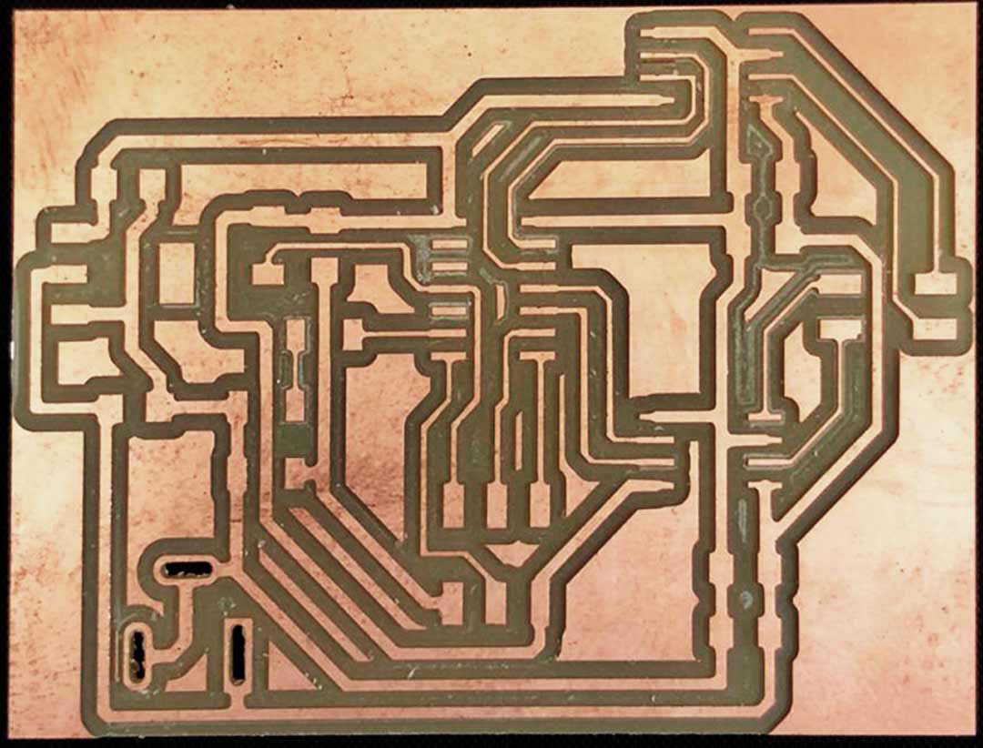
The outcome of this processes is a set of images that can be translated to a g-code for milling the board or it can be printed to be transfer on the cupper plate.
KiCAD
I start a project in KiCAD. One of the first complex task was installing the necessary libraries in order to start designing. The good part was that the fablab team already made a custom library with the component that we have in the inventory so this made the process much easier and smother.
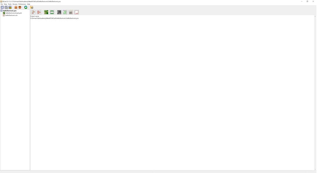
Fig01- opening a new project in KiCAD
Then I opened the symbol editor
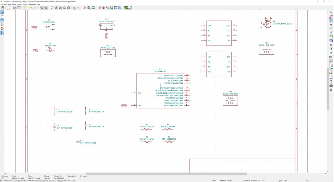
Fig02- Placing the component that I need for my design
After that start making the connections based following orders
- powers supply
- powers in the boards
- actuation
- data
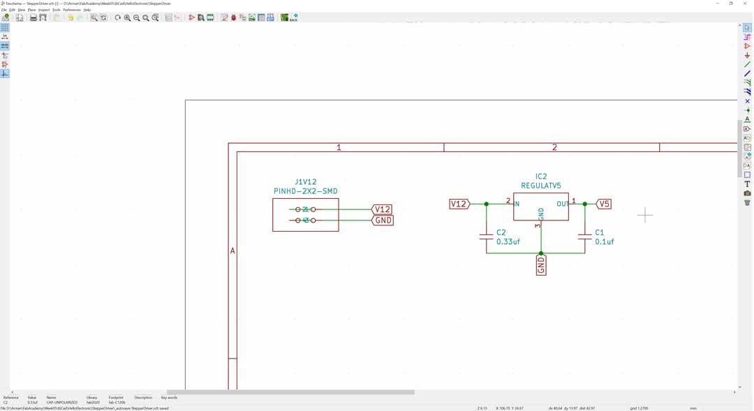
Fig03- Power supply symbol sketch
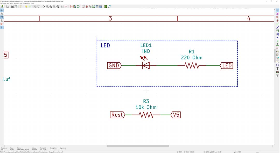
Fig04- Led and reset button connections
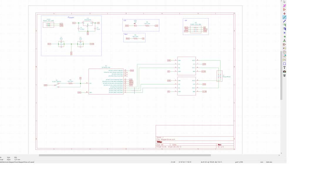
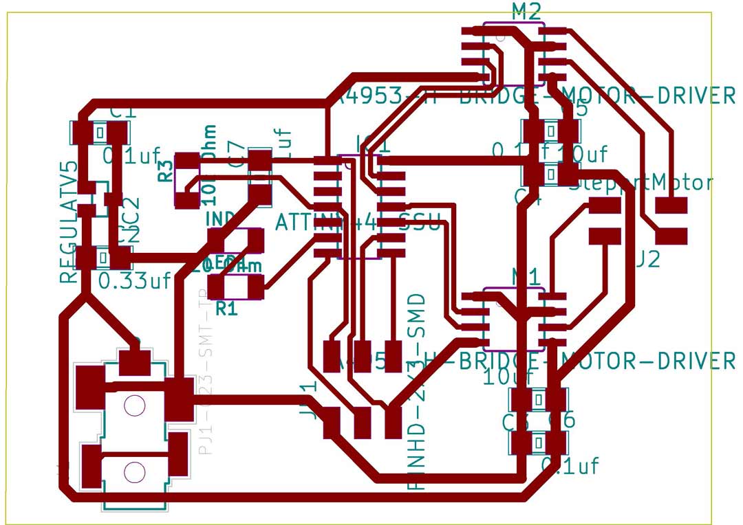
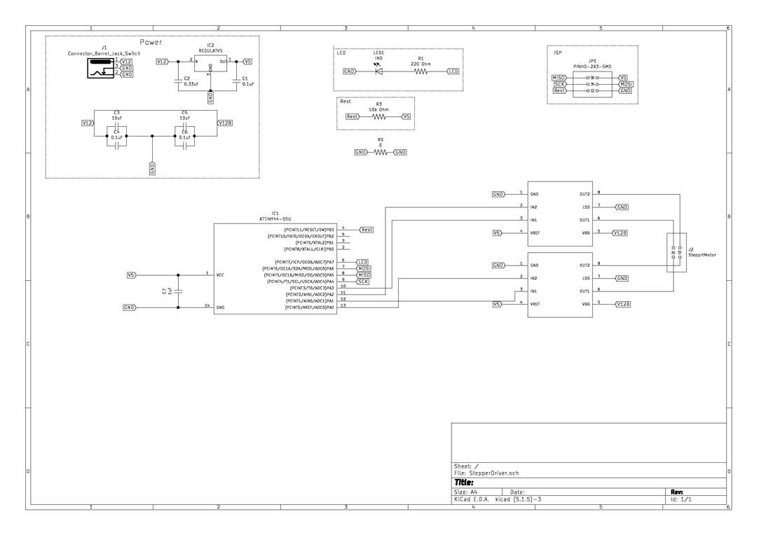
Fig05- overall symbol schematic
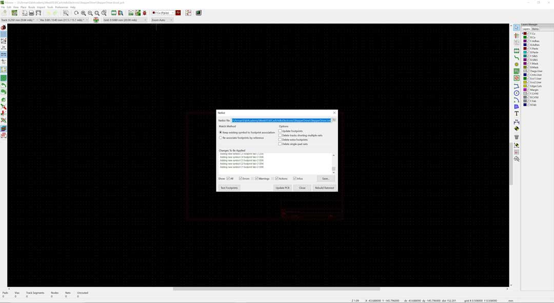
Fig06- Load the Net from the schematic
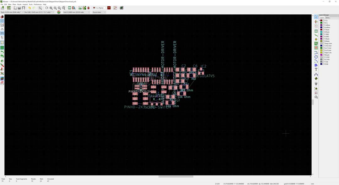
Fig07- Loaded footprint based on library
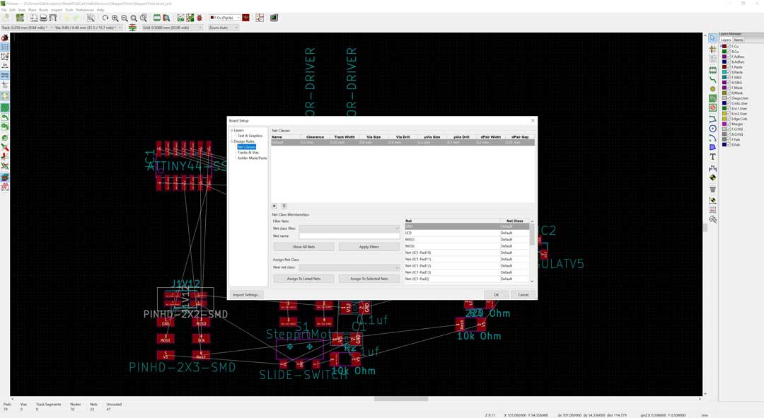
Fig08- Board setup
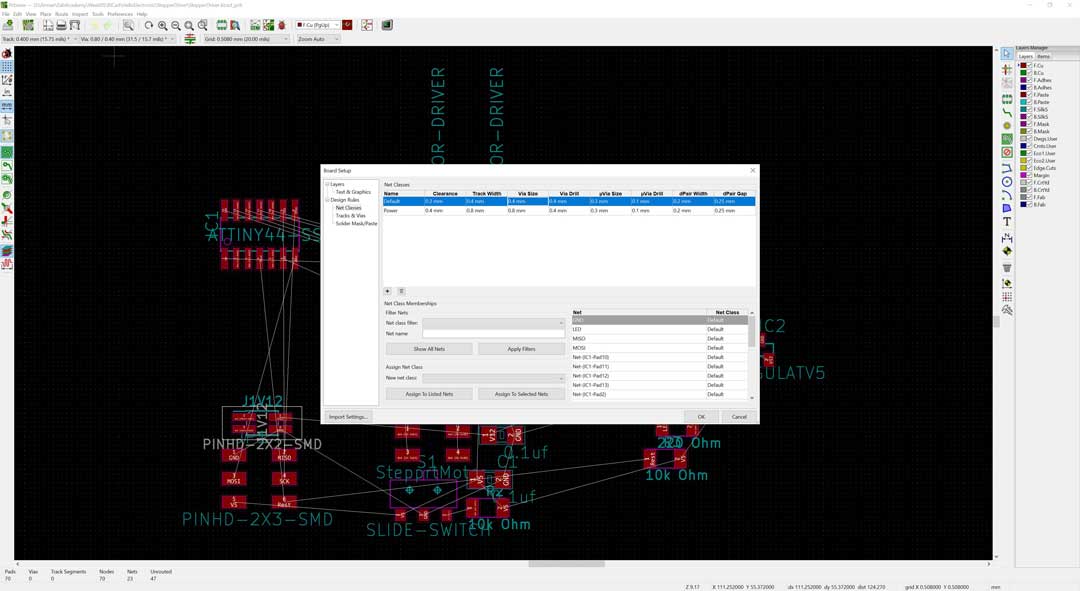
Fig09- Adding the specific trace for power since I have 12V motor to run
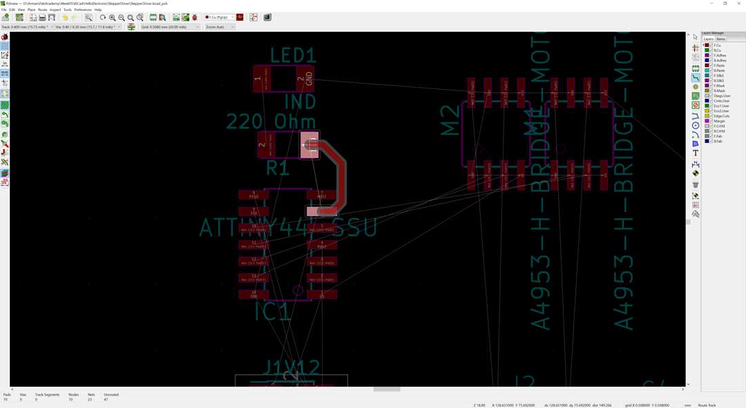
Fig010- Draw the trace base on the net guides
I think this is the hardest part of the whole design.
- Quick tip: use the caliper while you placing the component it will give you a rough estimation of how much space you can occupy base on the PCB board size.
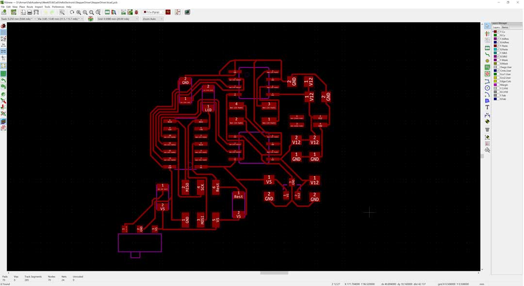
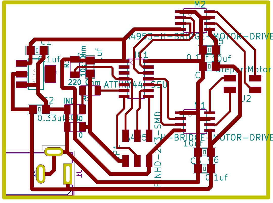
Fig11- Finish the trace and placements
TAAADDDAAAAA !!
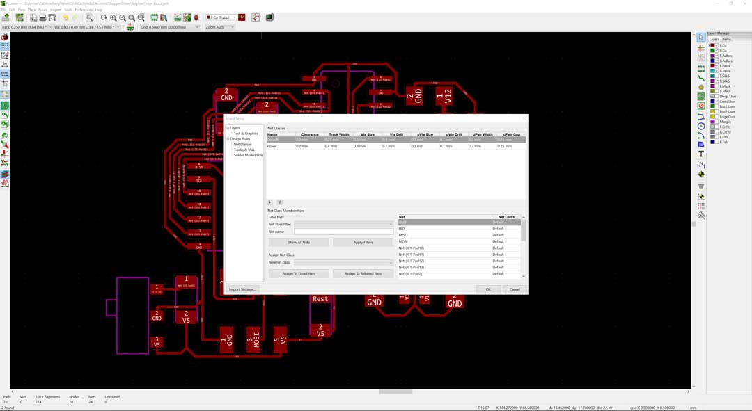
Fig11- Remembered to set the power trace !?
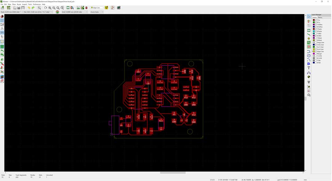
Fig13- Finish out cut design
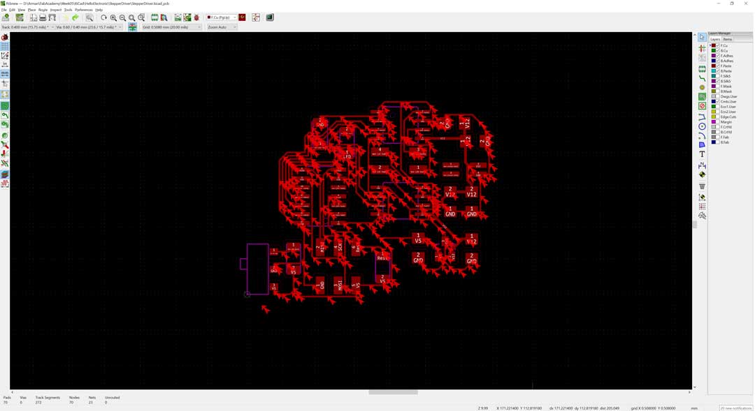
Fig11- Ok it all wrong!
I did a mistake
I set the trace size after I finished the drawing them. the top part documentation is from my redoing the footprint design but I have not finishing it yet.
Finally I finished the design of the trace.
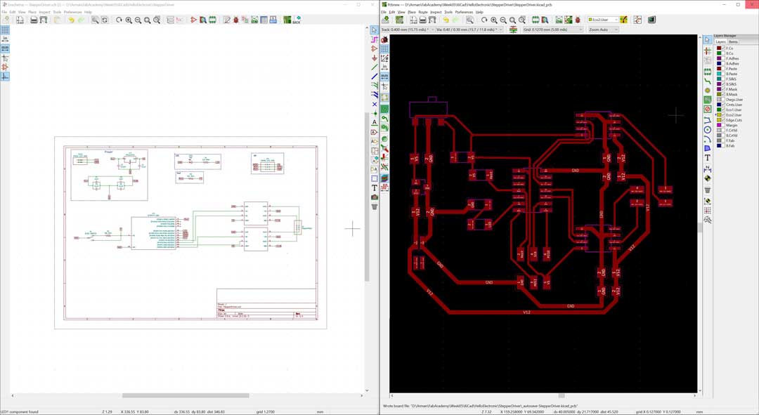
Fig11- Finishing the design
So after doing and redoing the trace design here is couple of tricks that I have learned.
- Firs consider loops of grand and voltage all over your board since you have to reach them to all of your components(almost)!
- Group the traces based on your sketches help a lot for the connection.
- start from processor since they have limited space and many legs to connect.
- I love using under the components for passing the trace but be aware of the clearance. (which you probably set at first if you follow up my mistake earlier on!)
- remember some of the connections can be adjust later in the code so change the connections on your sketch if you faced some difficulties(Don’t forget to save your net and update the net in the trace design mode)
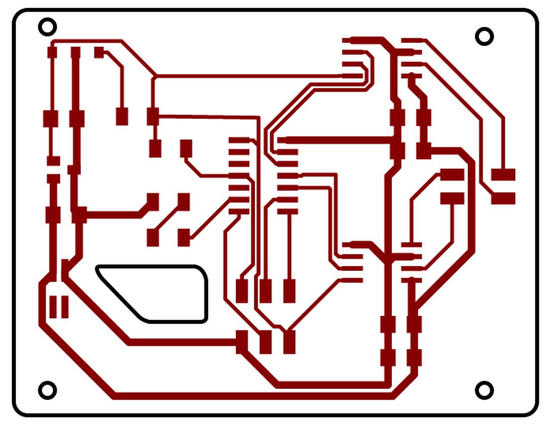
Fig11- design the outline cut!
At the end I found out it is easier to design the outline of the board in a 2D drawing app. I added some holes for mounting the board on my machine and a finger tip place for holding it.
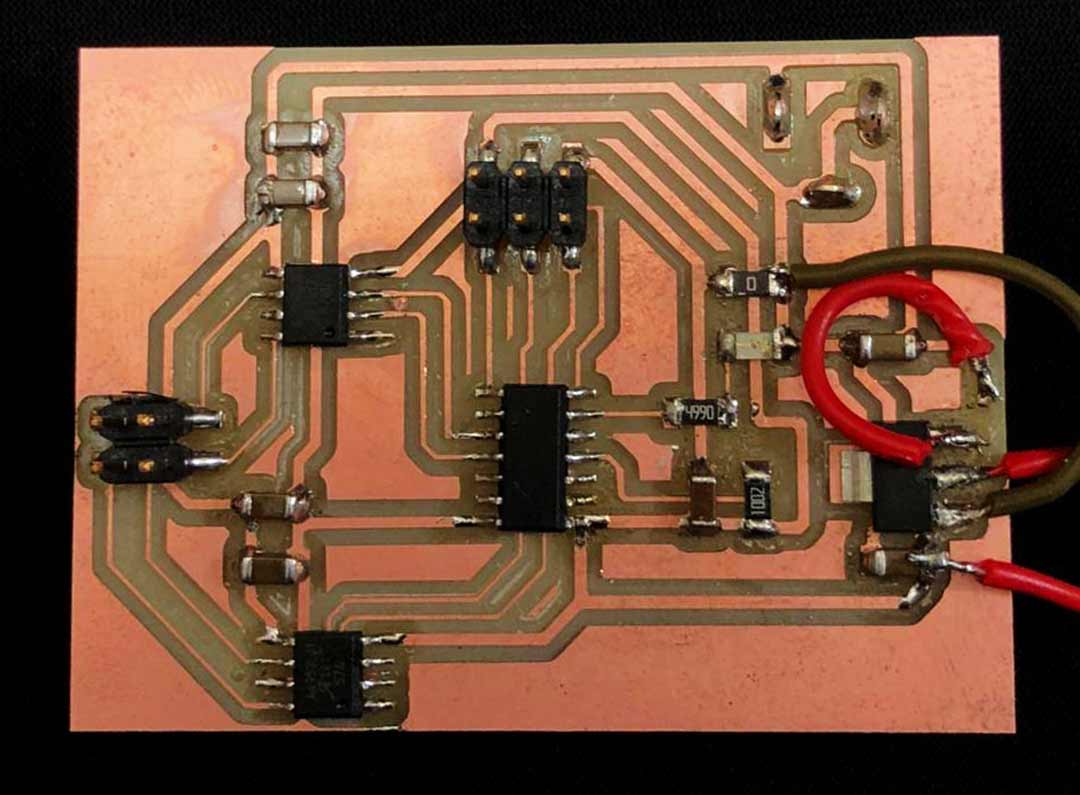
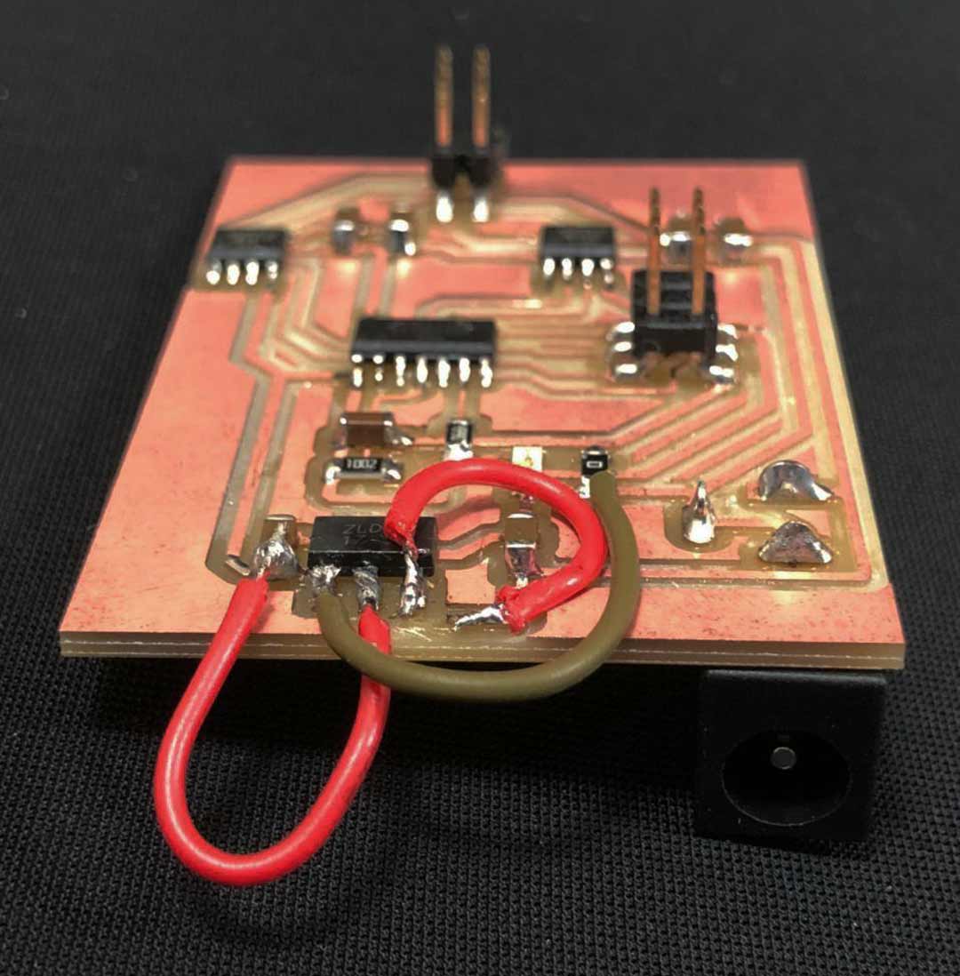
After some review with instructors I re-design this PCB. the main part that I had to adjust was the power management. I add a power jack instead of terminal.
But then I realize that I the regulator that I have used is for 100mA and the stepper motor will need more current. Thus I had to update the schematic and the PCB design.
After making CNC the file I realized that the footprint of the regulator connection is not matching with the datasheet of the component that I want to use. therefore I had to insert some jumper to fix the error.
Video1 The process of the milling
One of the issue that I have with designing the boards is choosing the right capacitors and resistors. I am sure in electronic filed the do know how to calculate this but so far I am just using other designs or datasheet suggestion to handle this issue.
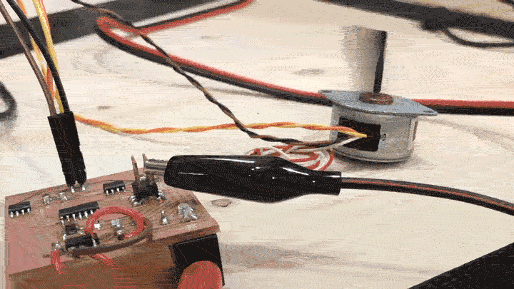
Make it work
To make the stepper motor works I have used Neil’s code to program this H-bridge. I have used arduino as ISP to program this attiny44(My ISP programmer is not working on my machine, windows10(2004) does not allow me to install custom driver on my device).
Files
You can download the KiCAD and the production files from following link.