Week assignments
Group assignment
- Use the test equipment in your lab to observe the operation of a microcontroller circuit board
Individual assignments
- Redraw the echo hello-world board, add (at least) a button and LED (with current-limiting resistor), check the design rules, make it, test it.
- 3D scan an object (and optionally print it)
Observing the operation of a microcontroller circuit board
You can find documentation about our group assignement on our group page.
To test the operation of a microcontroller we used a multimeter. We first mesured the voltage from VCC to ground. We could confirm the 5V.
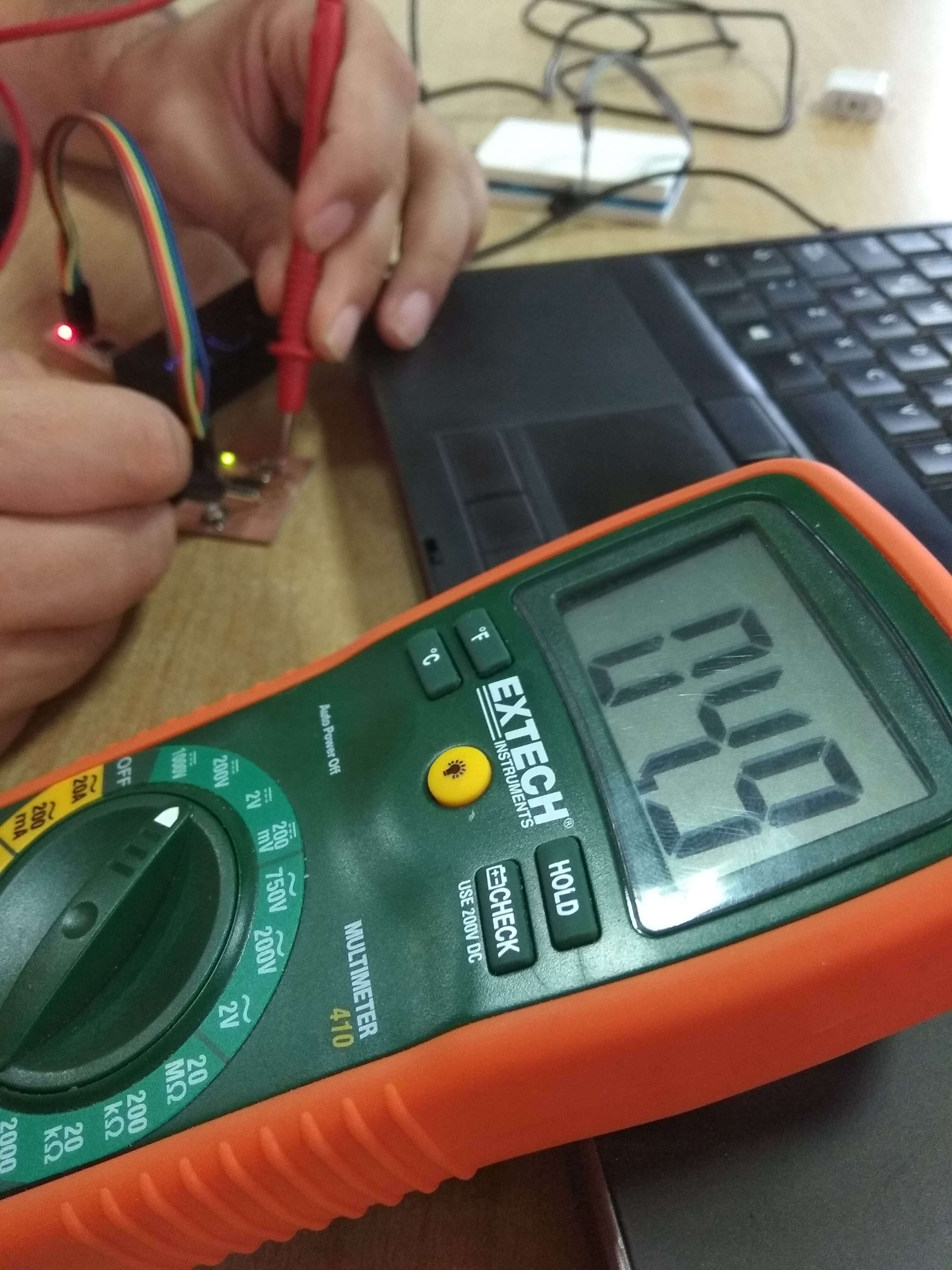
Then we measured the variations of voltage around the LED caused by the blinking.
Redrawing the echo hello-world board
KiCad - Eeschema
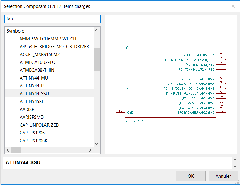
First of all, I had to add the fab component library that is accessible here.
Then, I had to select the components and place them on the grid. The picture below is an example with the selection of the ATTINY44 microcontroller.
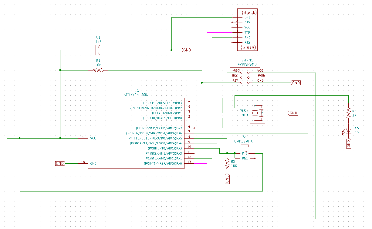
After having placed all the components on the grid, we can connect them. For that, I helped my self with neil design that you can access here. In addition, I add a 6mm switch and a led.
This is how it looks when every components are connected.
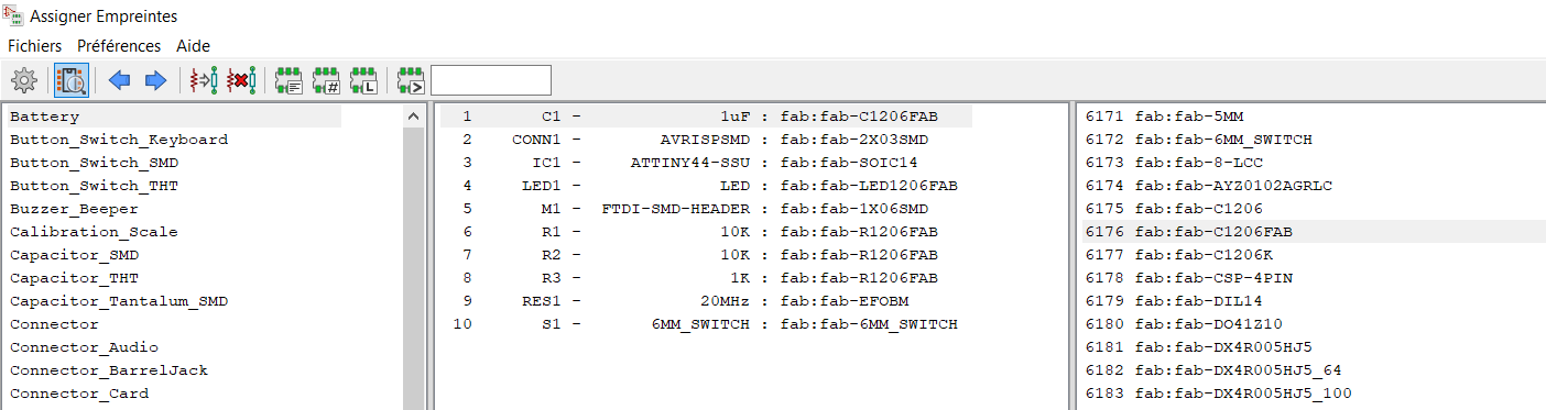
Before being able to go to PCB new, we have to annotate our design and assign footprints to each component. To do that we first have to load the fab.pretty library and then double click the corresponding footprint for each component.
Once all of this is done, I can just save the netlist.
and go to PCBnew. </p>
KiCad - PCBnew
In PCBnew, I have to draw the actual design of the board using the footprint of every component.
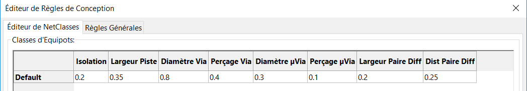
I first checked the design rules but kept them by defaults.
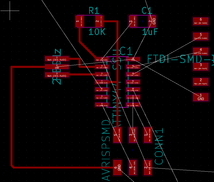
When the software opens, every component are placed in the center. I had to move them, turn them until it looks like I can find a way to link them.
Once it is done, I can start to link them. Here is a picture at the middle of the process. The white lines show what components have to be linked.
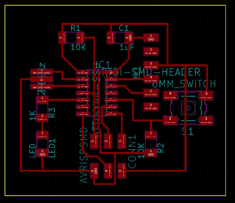
At the end of the process I went to edge.cut to delimitate my PCB. Here is the final result.
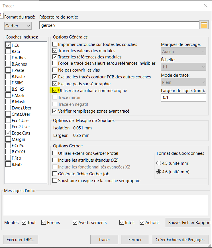
I now have to export my traces to be able to setup the milling job into FlatCam. To do that I first define an auxialiary axis then I use the plot option. I untick every layer I don't want to just keep F.Cu and Edge.Cuts. Plus, I tick the option "use auxiliary axis as origin".
And this is all for KiCad. I can now go to FlatCam. My gerber files are accessible here.
Preparing the milling job
First thing is to open the gerber files into FlatCam and generate the geometry with the tool diameter and the number of passes specified. This is what it gives me.
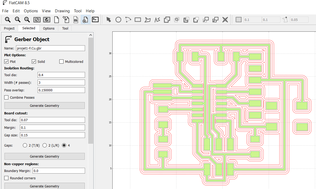
Before getting this result I had to do some troubleshouting with routes getting to close to other routes or components. And if you have a good view, you might see that there is still an error onto the AVRISP connector between Reset and SCK pins. This one I forgot before sending my file to the milling machine. I have been able to correct it using the machine manually.
I could have avoided this error by changing the clearance in the design rules of KiCAD. We didn’t change it at first because we assumed half of the end mill diameter would be enough.
Also, we didn't know it for my PCB but I could have tick "combine passes" to make only one .nc file. Anyway, we use a stepcraft for a PCB milling machine and it is very slow. So I did only one pass.
Milling and soldering
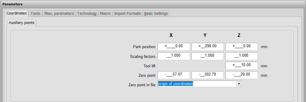
This process is the same as in week5. We only discover one new options. We are using two nc files to do the trace milling and the edge cutting. Every time we had to set a new zero despite the definition of it into FlatCam. Actually to take it into account into FlatCam, you have to go to Parameters-->Coordinates and then change "Zero point in file" from "bottom left" to "origin of coordinates".
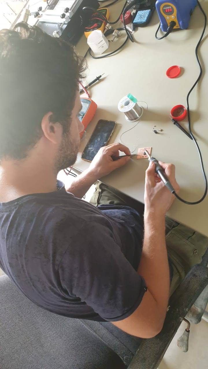
Then I went back to soldering.
Testing the board
We had to do some troubleshooting with that part. First we tried with an Arduino and then with an ATTINY45 ISP (Brian) on linux. With both of them we had the error :
avrdude: Expected signature for ATtiny44 is 1E 92 07
         Double check chip, or use -F to override this check.
One work around with ATTINY45 is to keep the jumper.
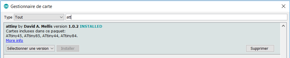
Then we tried with the ATTINY44 ISP on my windows computer. First I had to install the drivers of the board. And I also had to install the board into the arduino IDE --> Tools --> Board Manager --> Attiny.
Then I had to configure arduino IDE.
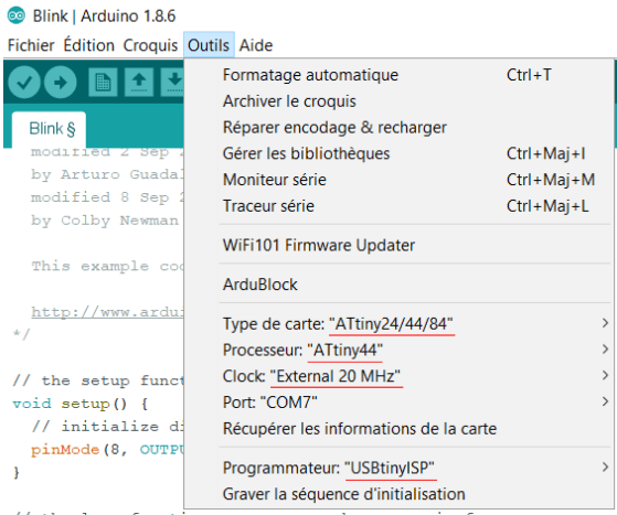
Once setup, I opened the blink example and just had to change the LED_BUILTIN parameter to 8. Then I uploaded it and there is the result.
I have also been able to test my button by using the button program example into arduino IDE.