Fab Academy 2020
Introduction
This week Assignment is to make an in-circuit programmer by milling the PCB.This week we need to build our own ISP(In-system programming),also called in-circuit serial programming (ICSP).we are building a Programmer for RISC-(Reduced Instruction Set Computer)based Microcontrollers, it's a Popular Architecture used in Controlers. Arduino uno is a Popular Development Board based Atmel-328P MicroController's and it's comes with in-built Circuit Progarmmer.
To program a chip, we will need a special programmer which reads commands from USB to drive the SPI lines to program the chip.SPI stands for Serial Peripheral Interface and is a way for microcontrollers to communicate with each other or with the outside world. It's also called 3-wire sometimes because it uses three wires to communicate.
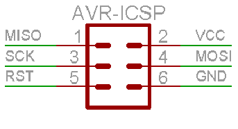
- VCC - Postive Voltage
- GND - Ground
- RST - Reset Pin
- MISO- Master In Slave Out
- MOSI- Master Out Slave In
- SCK - Serial Clock
In here MISO,MOSI, and SCK are the most important.
In SPI system , there will be a main Module acting as a Master and peripheral acting as Slave. When master need to send some data/need to communicate with slaves, the MOSI channel will be active based on the SCK(Serial Clock),so the communication will happen in given Clock time , all the slave will act as a Input and Master act as Output so the Master can give instruction ,like this if the slave need to communicate to the Master they can use MISO that's means the Master can act as Input and Slaves will act as Output, therefore Slave can give Feedback to the Master .
What i did?
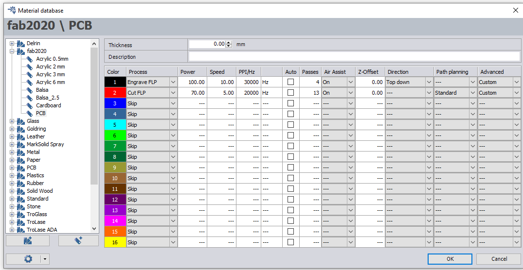
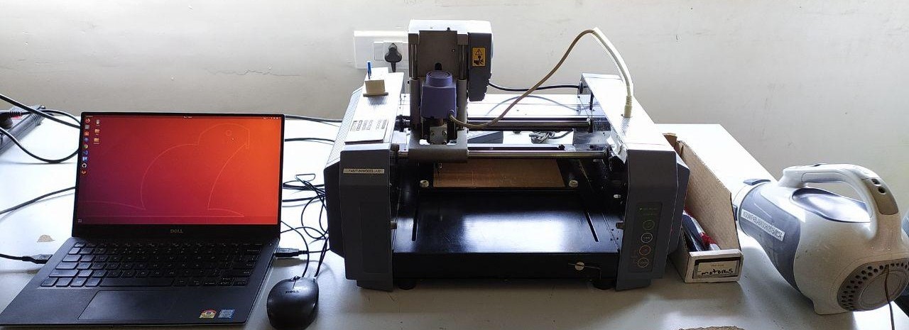
Roland Modella MDX20
The main goals for 4th week conists of electronic production where group assignment conists of machining the line test using the 1/64 bit to see the the maximum resolution. The machine used for the milling process is roland mx20
We got all the PCB designes so no need to design one,after the design we need the Fabricate the PCB, there are Several methods.like PCB chemical etching ,Photoresist PCB laminates and PCB Machine Milling. In here we are using PCB Milling, milling is the process of removing areas of copper from a sheet of printed circuit board material to recreate the pads. We will be focusing on the Milling process.
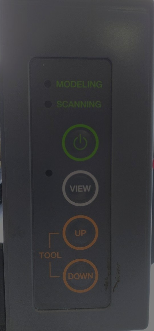
The main components of the machine are a moving head which is numerically controlled a bed where is PCB board is placed and control panel with essential components.It can be used for scanning and also milling.The machine is controlled using mods which can be used for various machines, and vaccum pump to remove debris formed.
Machine interface where the milling head can be moved in different directions.
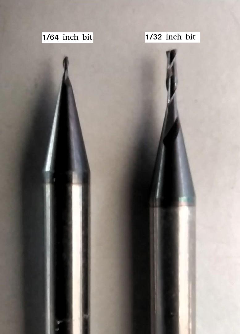
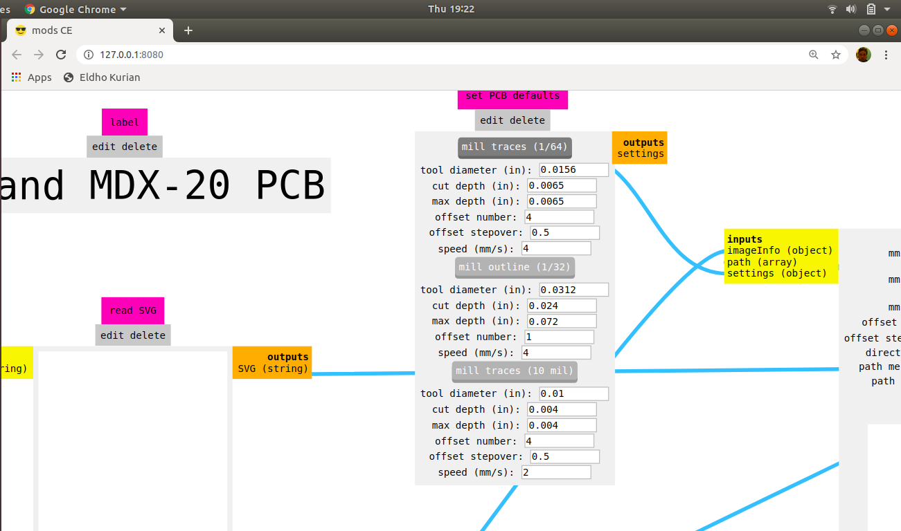
Below the drillbits used for the milling process can be seen where one is 1/32 of an inch and the other 1/64 which when converted to mm are 0.0312 and 0.0156 mm. 1/64 bit is used to make the trace and 1/32 is used to mill the boundries.
Group Assignment
The group assignement for this week is explained in detail in the group page. To access the group page click here.
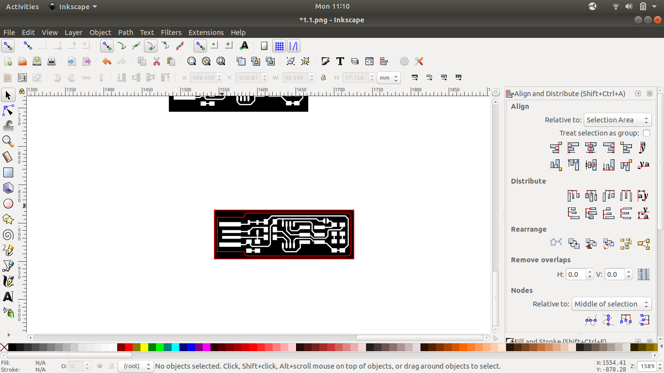
PCB milling
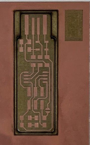
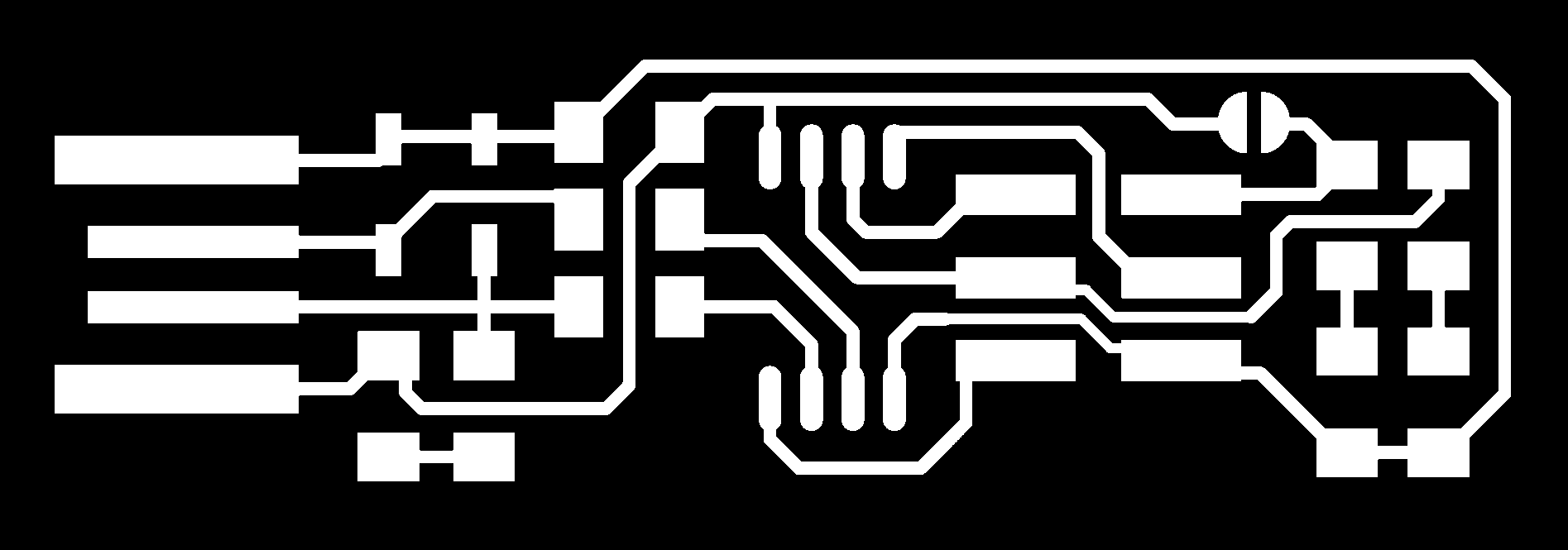
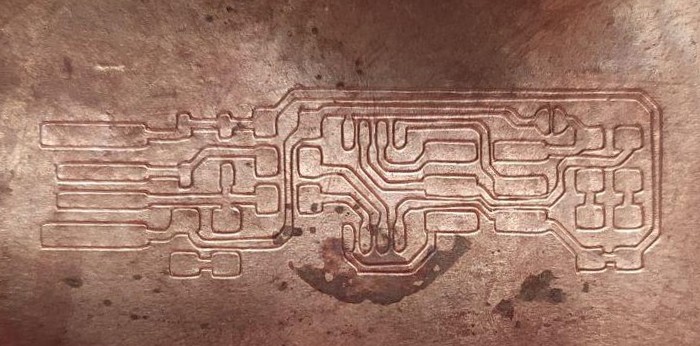
After doing the group assignment basic steps which we should be carefull about are known further.The below shown image downloaded from fabacademy database shows the PCB pattern which is needed to be milled the black portion is milled away using 1/64 bit and the outline is cut through the PCB using 1/32 bit.

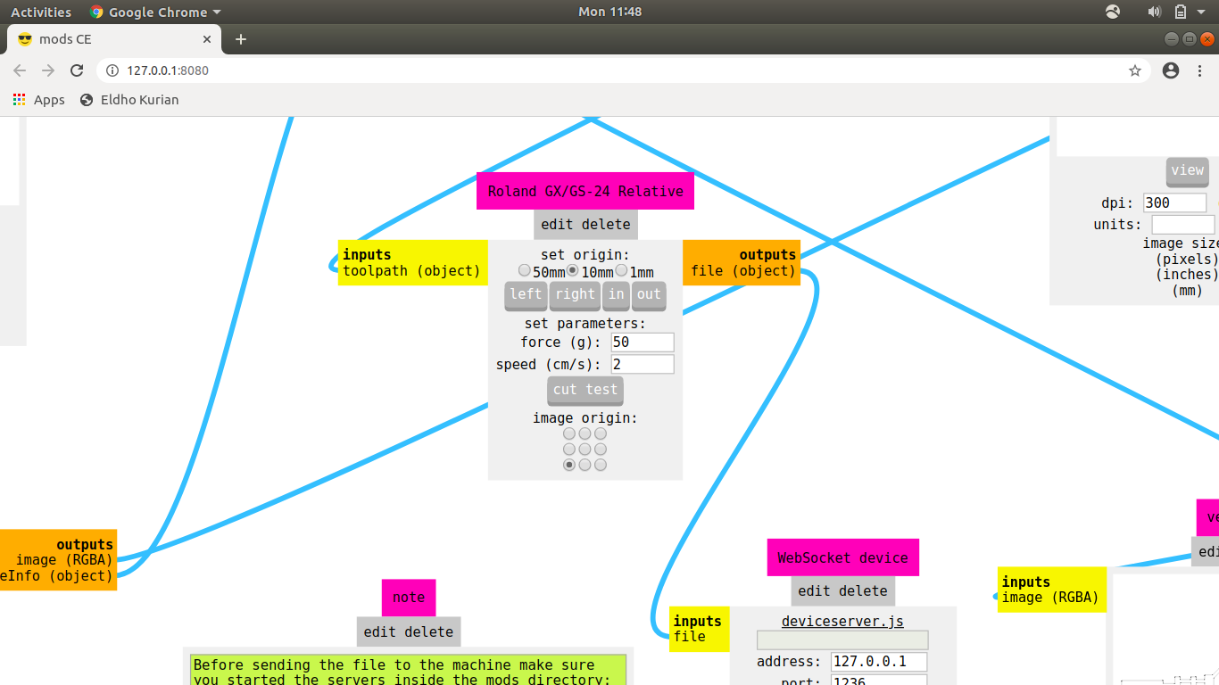
The process starts with mods and the file is loaded using the following steps. Before doing the milling we should be sure of the bit to use. For trace 1/64 bit is mounted on to the mill head carefully.
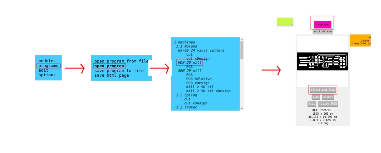
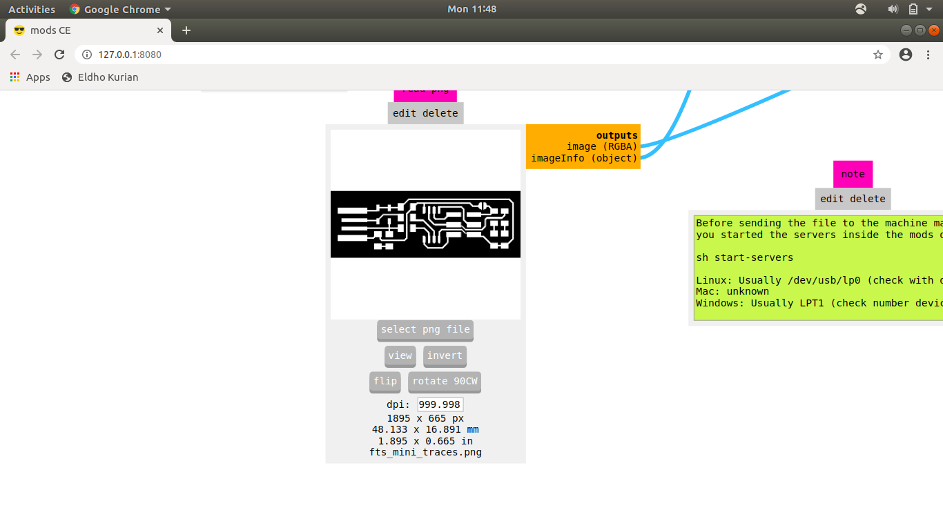
The file is loaded as png file.For trace mill trace 1/64 is selected and the path is calcualted after changing the required parameters. Origin is set and the file is sent to cut.Similarly in case of boundary cut the bit is changed to 1/32 and the boundary png file is loaded to MODS.
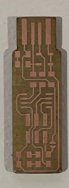
After tracing is done by removing copper a circuit outline is formed and the now the bit needs to be changed and 1/32 bit is used to cut out the pcb circuit from the board.
Soldering
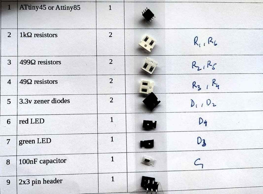
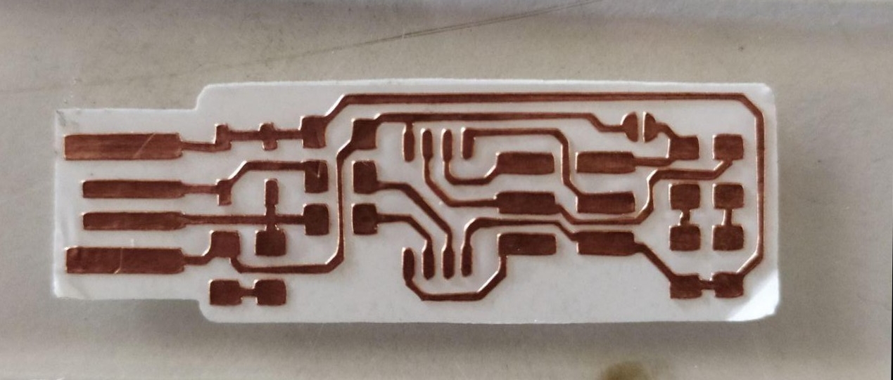
For me its first soldering experinace. First i collected all the necessary components needed and cleaned the milled pcb board to avoid any unnecessary fragments.
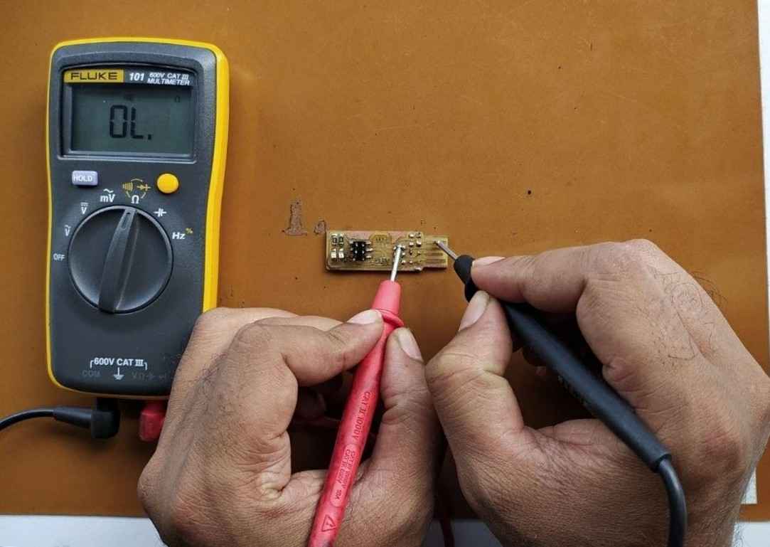
It is a good practice to check the connectivity of the traces using a multimeter for seamless results.
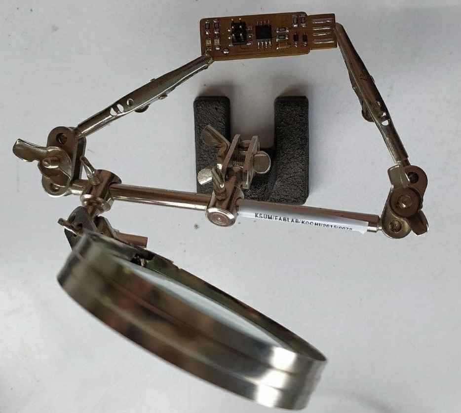
The setup used to hold the board conists of various fixtures which can be fixed on the board and consists of a lens which is used to view the components clearly
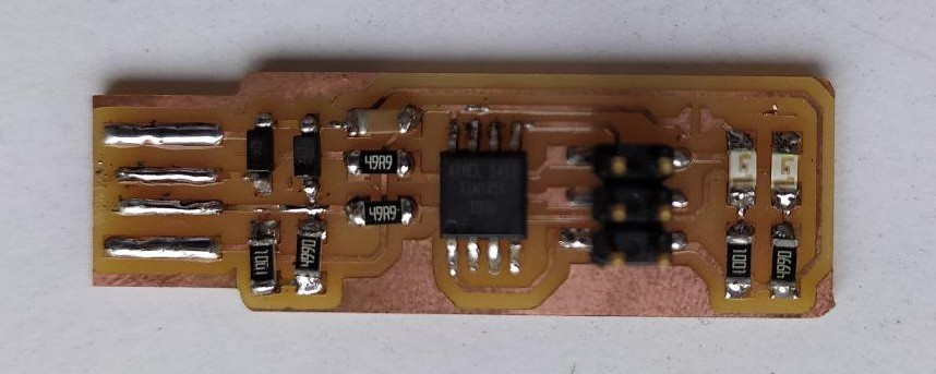
After the soldering process the PCB board looks in good shape it needs to be programmed for using it as an ISP.
ATiny 45 programming
For programming AVR neccessary softwares should be installed
So we would need
- Avrdude (for programming AVR microcontrollers)
- GCC (to compile C code)
First to install the GCC software the following codes should be entered in the terminal. The GCC installation instructions are available here.
sudo apt-get install flex byacc bison gcc libusb-dev avrdude
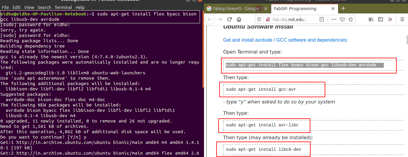
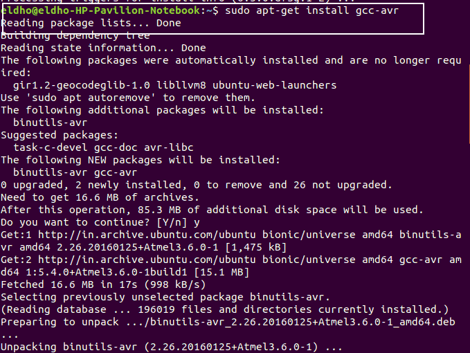
sudo apt-get install gcc-avr
sudo apt-get install avr-libc
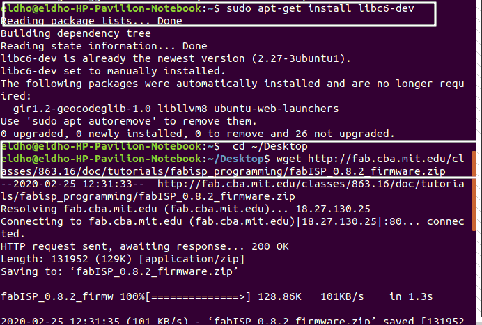
sudo apt-get install libc6-dev
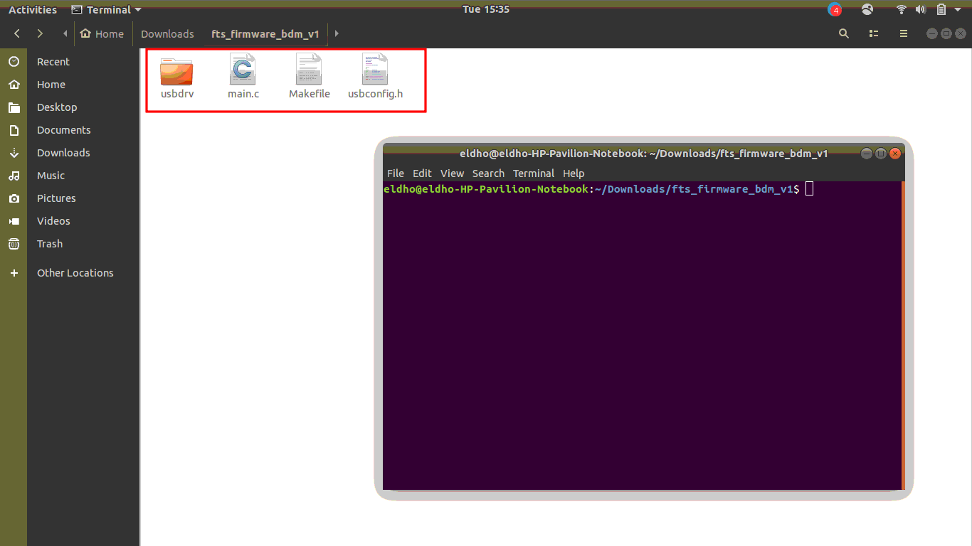
Next steps are to download and unzip the firmware. Change the directory to desktop and the unzip process starts by entering the file link to the terminal.
The process is done by entering the follwoing commands
cd ~/Desktop
wget http://fab.cba.mit.edu/classes/863.16/doc/tutorials/fabisp_programming/fabISP_0.8.2_firmware.zip
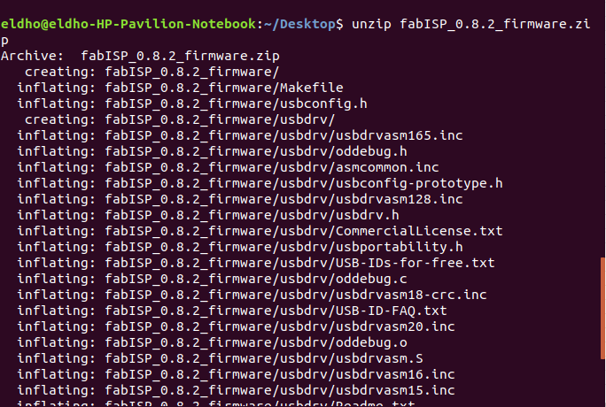
unzip fabISP_0.8.2_firmware.zip
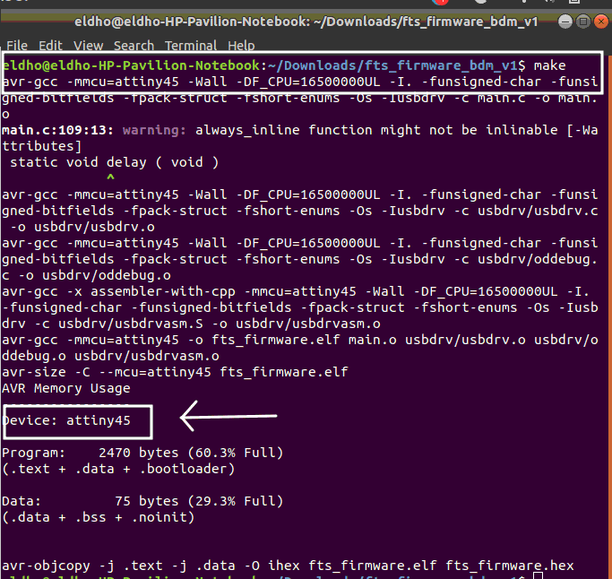
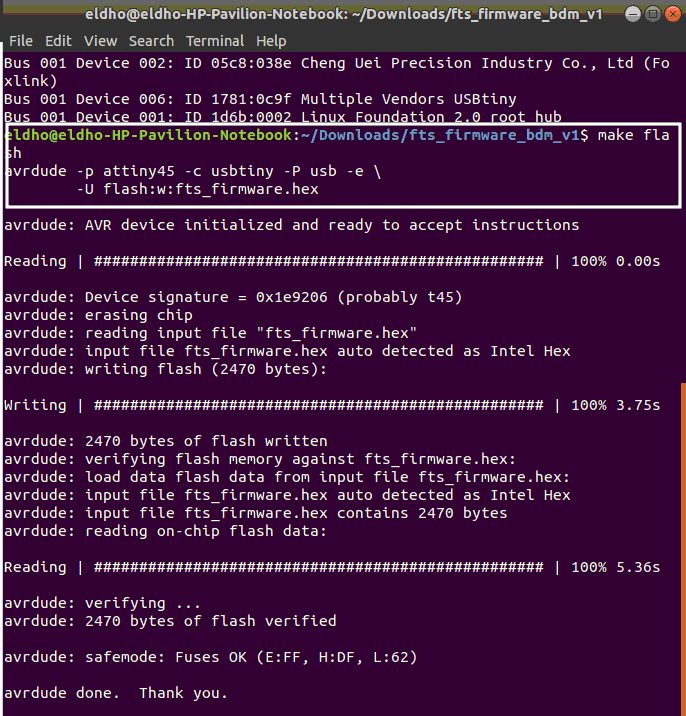
Once in the directory type ‘make’and click enter. This will build the .hex file that will get programmed onto the ATtiny45. When the command completes, you should now have a file called fts_firmware.hex.
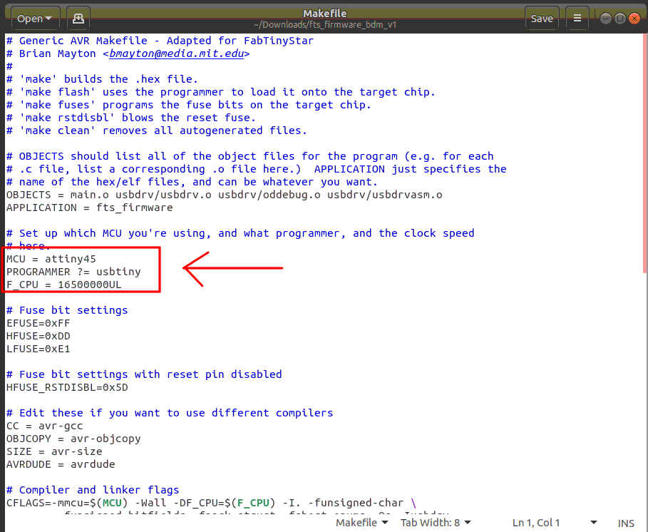
The make file of the firmware assumes that you are going to use a programmer in the usbtiny category (another fab ISP). If you're using a different programmer, first figure out what avrdude (the programming software) calls it.
Edit the file called Makefile. It is important to use a text editor intended for programmers. Near the top of the file, find the line that says:
PROGRAMMER ?= usbtiny change usbtiny to whatever programmer you're using.
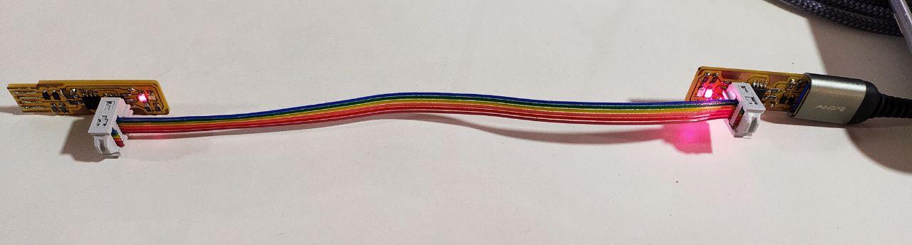
Plug the board into a USB port. USB2.0 is preferred over 3.0 if you have one, and use an extension cable so that you do not put strain on your board especially if your port is upside down.Connect the programmer to the ISP header on your board. Note that there are two different orientations in which you can connect the cable; it is imporatant that you get pin 1 in the right place. Pin 1 is the MISO pin and it should be connected to the MISO pin of the board you are programming.
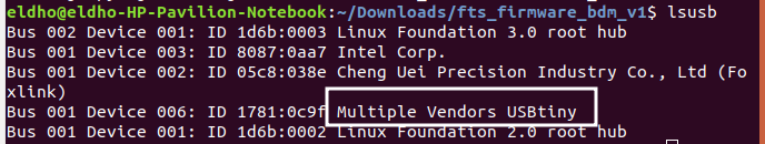
Type lsusbIn terminal and ensure the device is identified
After in the terminal run the command ‘make flash’. This will erase the target chip and program its flash memory with the contents of the .hex file you built before. You should see several progress bars while avrdude erases, programs, and verifies the chip.
Detailed debugging steps are provided in the FabTinyISP documentation page. Once you've successfully programmed the flash memory, it's time to set the configuration fuses:
- First, we'll set the fuses that control where the microcontroller gets its clock source from. This will allow us to check that the board works as a USB device, but it won't yet be able to program other boards.
- Only after confirming that USB works, we'll set the fuse that disables the reset pin and turns it into a regular GPIO pin. This will let the chip use the reset pin to program other boards, but will disable the ability for this chip to be programmed again.
Go to the terminal and run the make fuses command. This will set up all of the fuses except the one that disables the reset pin.make fuse
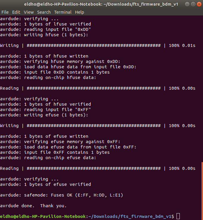
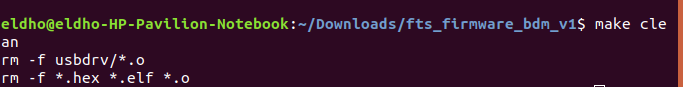
Make clean command removes all autogenerated file.We need to change the bit that will turn the ATtiny45's reset pin into a GPIO pin.This will disable our ability to reprogram this ATtiny45 in the future, hence make sure everything is working before doing this. Connect your ISP programmer to your board one more time, and in the Terminal run
Group Assignment
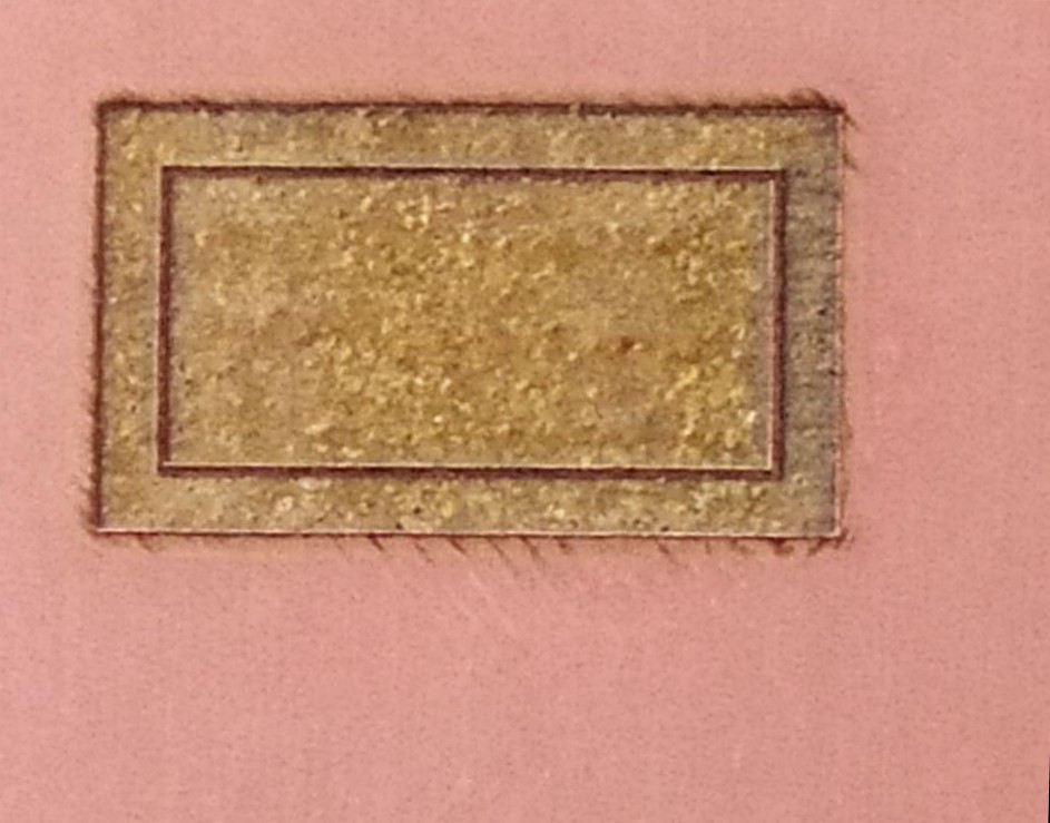
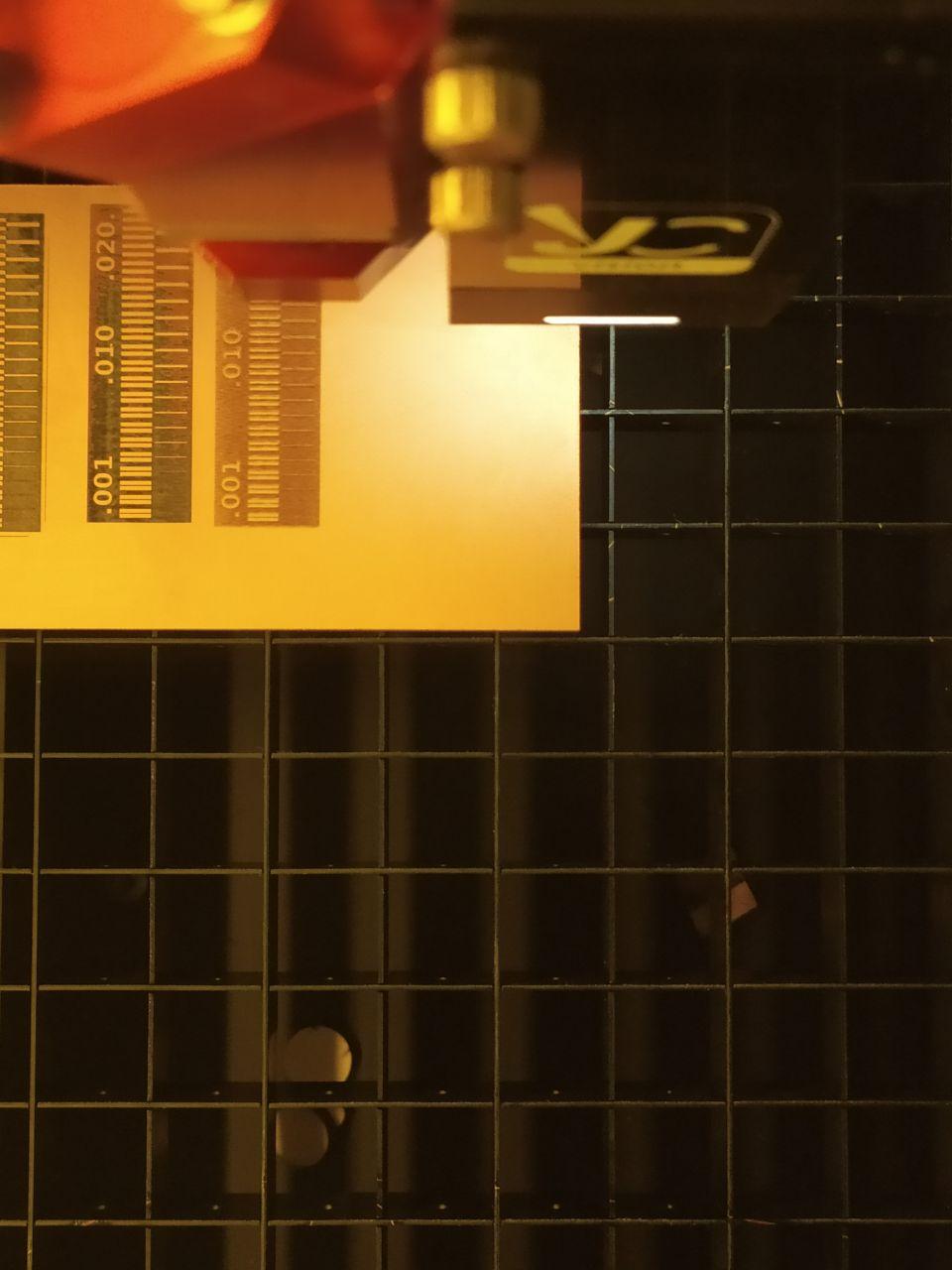
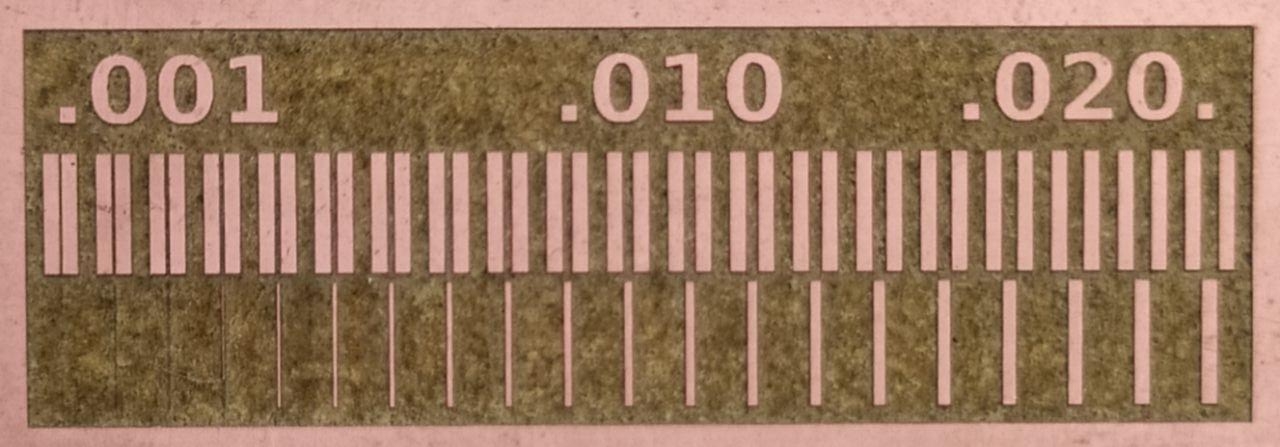
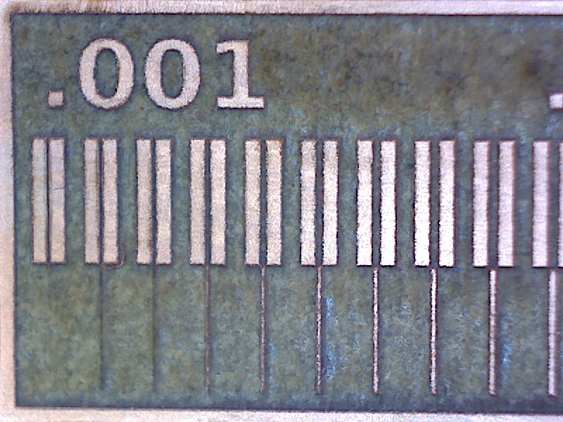
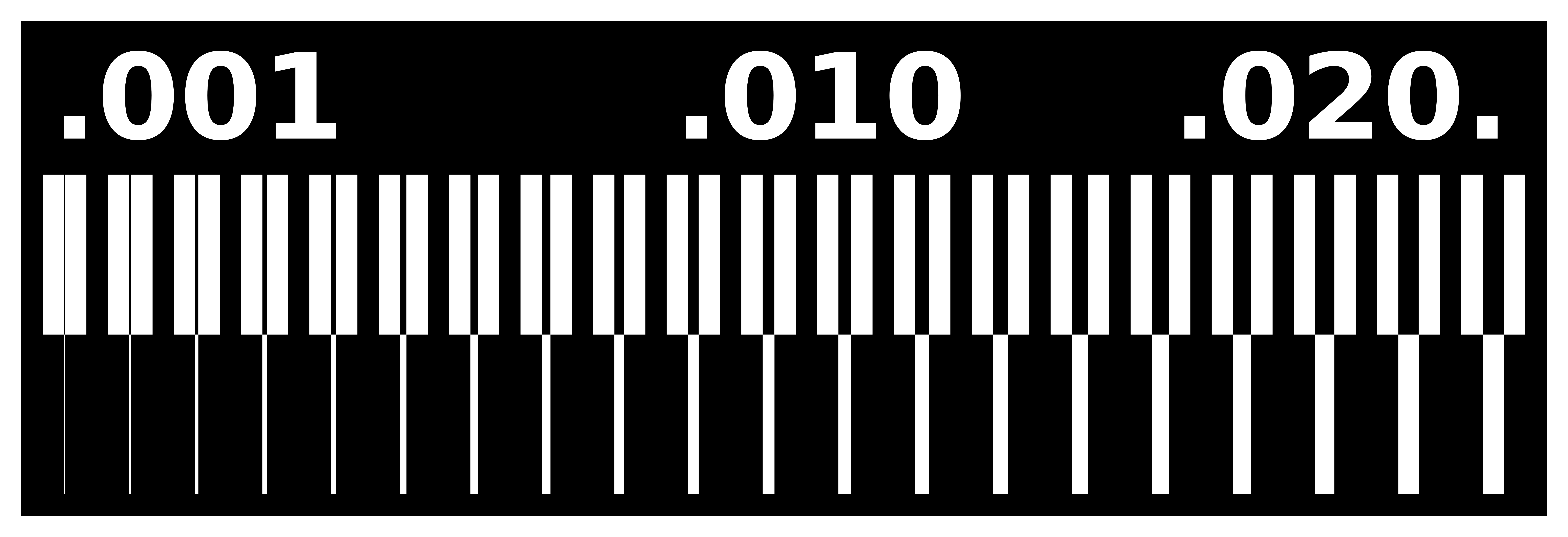
The below shown image which was downloaded from fabacademy database was used to do the linetest.
The above shown image was rotated 90 degrees using gimp application for milling purpose if the pixel of the image changes it can drastically adffect the milling process
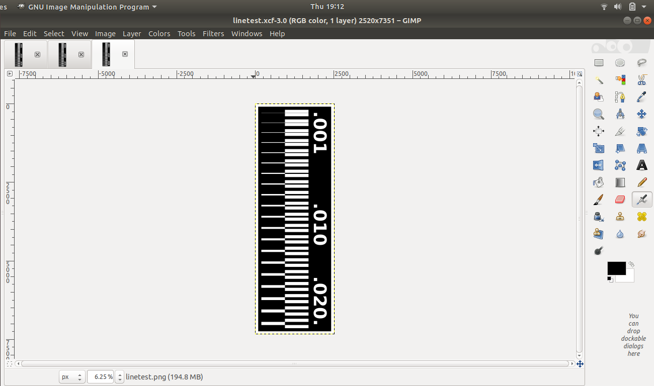
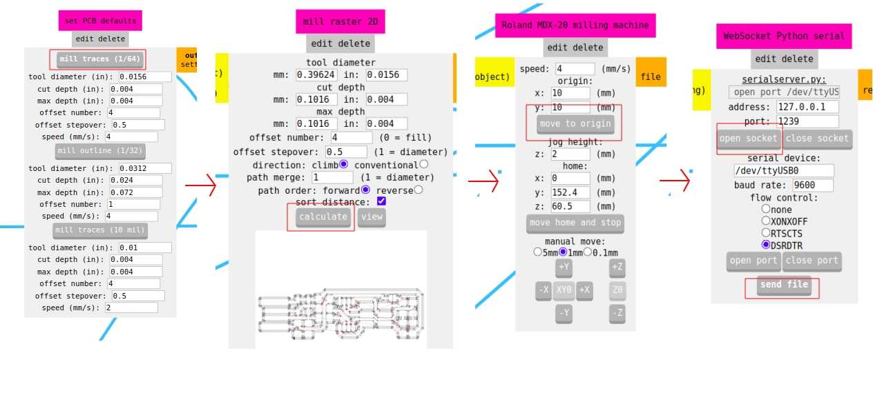
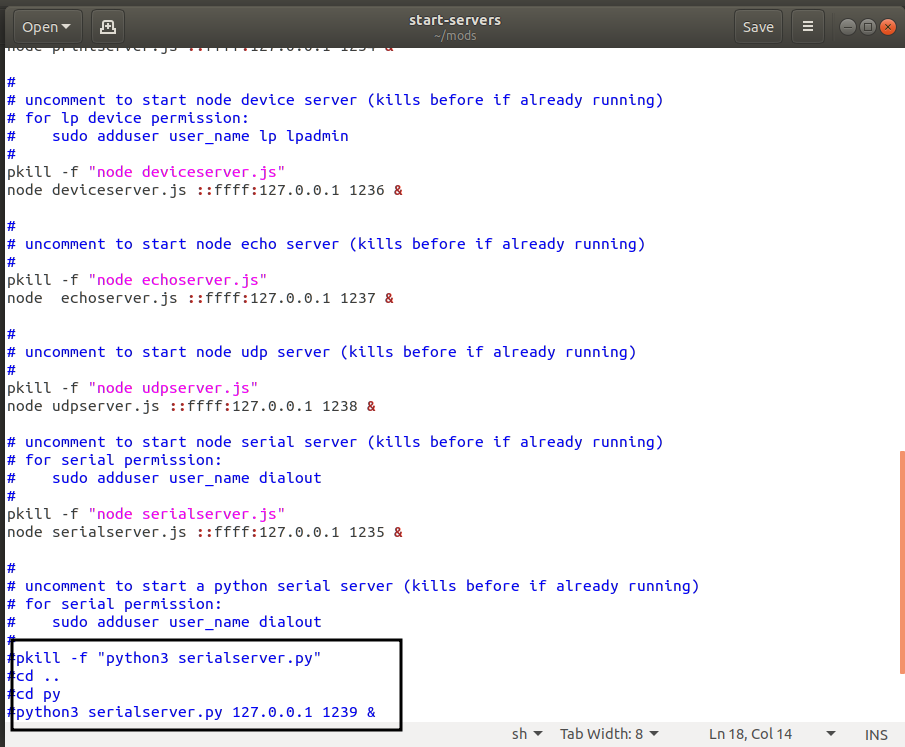
The milling process was condcuted using mods which is a usefull interface where the image is selected and the parameters are changed and the most important process is fixing the origin because when we use multiple bits it can affect the starting point of the milling. Below shown images are various steps from changes to be made in the starter package of mods where a editing of the commands make to access python.
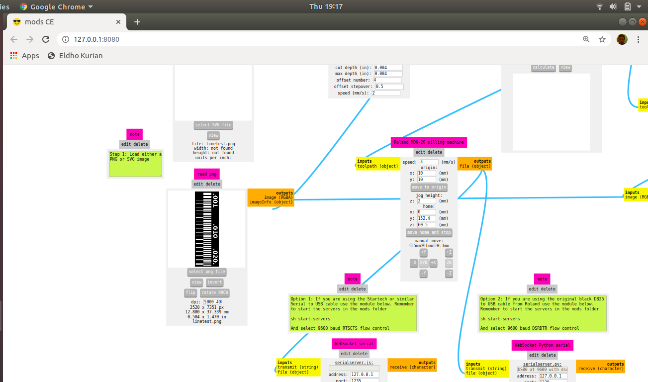
All neccessary paramters of the machine is already preset in mods and its can also be changed to our requiremnts.
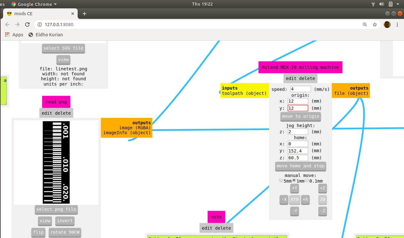
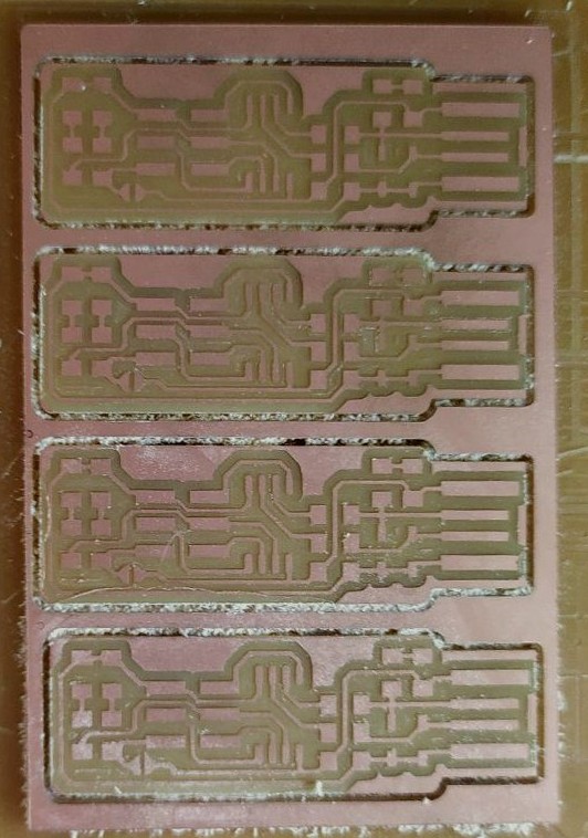
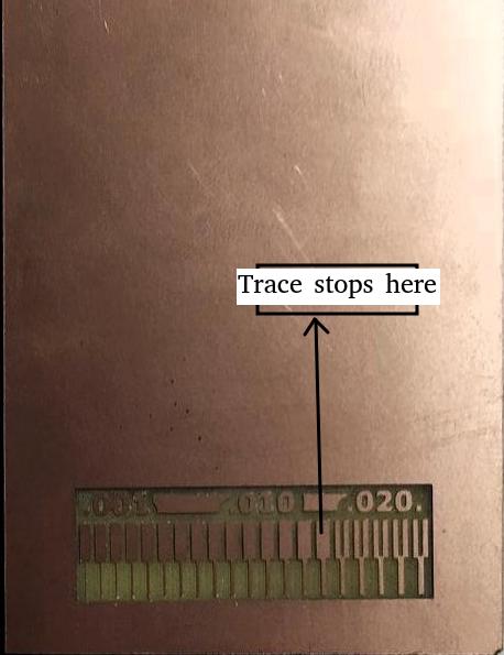
As shown below the tracing for linetest was done using 1/64 bit and it can be clearly seen that the bit stopsmilling beyond 0.016.So this is the maximum resoultuion which can obtained using this bit.
Vinyl PCB
Laser cut PCB