Fab Academy 2020
Introduction
In previous week of electronics board designs where given and mostly machine involvement of PCB milling was explored. This week the main aim is to understand how a prviously made design works and making effective improvements to the design. Since it would be hard to make a design from scratch a design file is given to study.
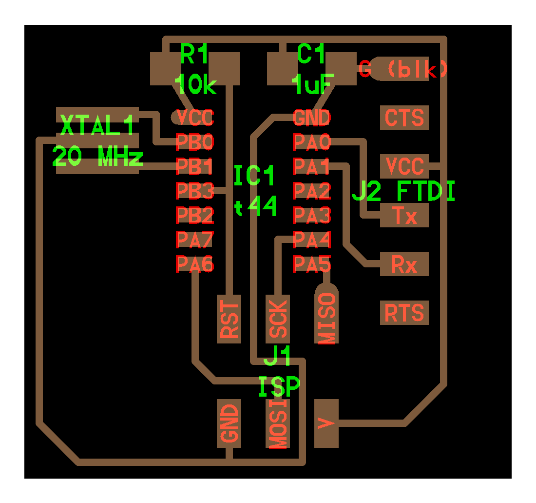
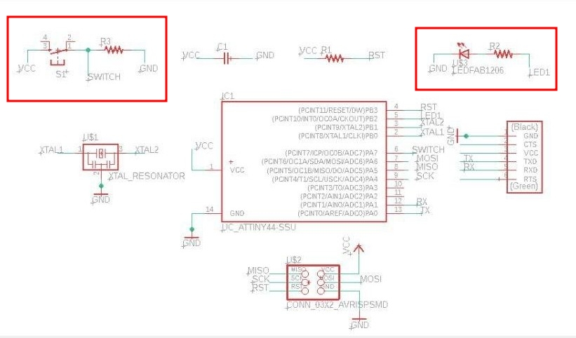
From this design file the components and its arrangement can be studied.We need to add an extra LED and and a switch to the circuit. to do that first we need to understand the function of each componets here and how a new component will affect the function of the circuit.
Group Assignment
The group assignement for this week is explained in detail in the group page. To access the group page click here.
Important Basics
Pull-up resistors
Pull-up resistors are resistors which are used to ensure that a wire is pulled to a high logical level in the absence of an input signal. Pull-up resistors are not a special kind of resistors; they are simple fixed-value resistors connected between the voltage supply (usually +5V) and the appropriate pin, which results in defining the input or output voltage in the absence of a driving signal.
Pull-down resistors
Pull-down resistors work in the same manner as pull-up resistors, except that they pull the pin to a logical low value. They are connected between ground and the appropriate pin on a device.
Resistor value
The appropriate value for the pull-up resistor is limited by two factors. The first factor is power dissipation. If the resistance value is too low, a high current will flow through the pull-up resistor, heating the device and using up an unnecessary amount of power when the switch is closed. This condition is called a strong pull-up and is avoided when low power consumption is a requirement. The second factor is the pin voltage when the switch is open. If the pull-up resistance value is too high, combined with a large leakage current of the input pin, the input voltage can become insufficient when the switch is open. This condition is called having a weak pull-up. The actual value of the pull-up’s resistance depends on the impedance of the input pin, which is closely related to the pin’s leakage current. However the resistance value for Attiny 44 is specified in its data sheet as 10KOhm to 20kOhm, We have opted 10kohm resistor for the pull-up.(thank you my friend lancy for this valuable informations.)
Eagle
EAGLE is a scriptable electronic design automation (EDA) application with schematic capture, printed circuit board (PCB) layout, auto-router and computer-aided manufacturing (CAM) features. EAGLE stands for Easily Applicable Graphical Layout Editor and is developed by CadSoft Computer GmbH. The company was acquired by Autodesk Inc. in 2016
Eagle is the most preferable because a lot of opensource projects are available in eagle .It is easy to use easly understandable and have a well back of active users .also it is free for hobbie projects and students.
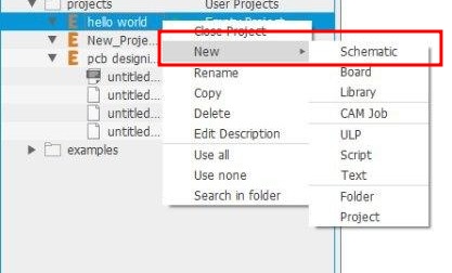
First we need to install eagle which is a sraightforward download. And to start with the design we should open a new project
command sequence : File => New folder => New project => New Schematic
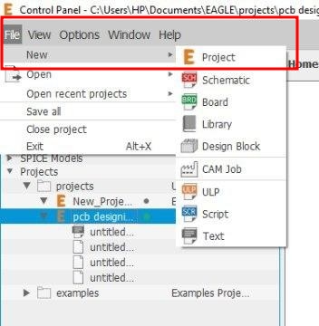
Since we need to create a schematic of the board connections-open schematics.
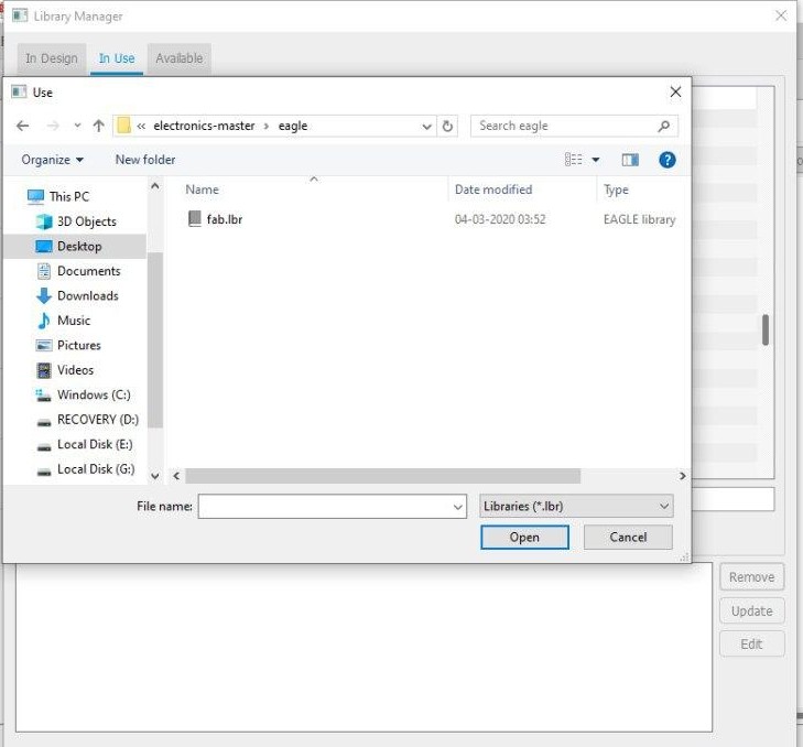
Even though there is component database in eagle. To use the components present in fablab repostary we need to update the library. Next step is to update the eagle library with the attiny circuit components. which is downloaded from fab directory.the directory can be downloaded from here
Extract and copy the fab.lbr file to the eagle library folder
command line : Library => fab.lbr => Update all
The components needed can be seen by typing the command add on the command window of eagle. The fab library is added in the section.
Next step is the find the neccassary components from the list.The required components can be placed one by one based on the circuit diagram.
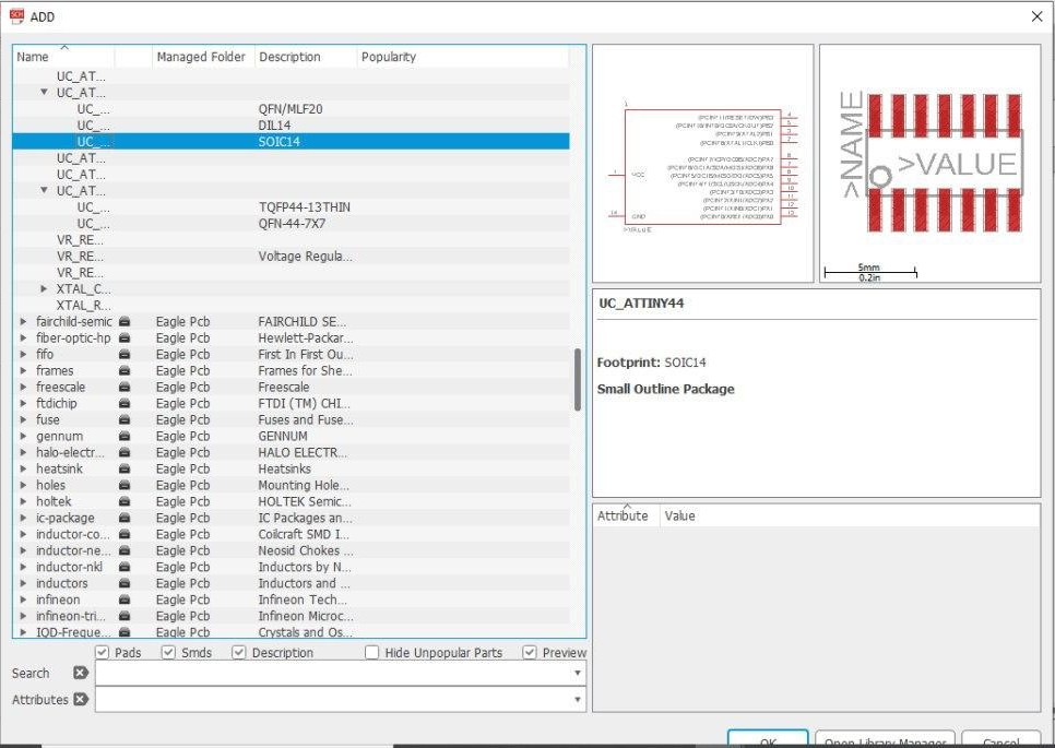
All the required components are selected and placed accordingly. The components are shown in the form of schematics.
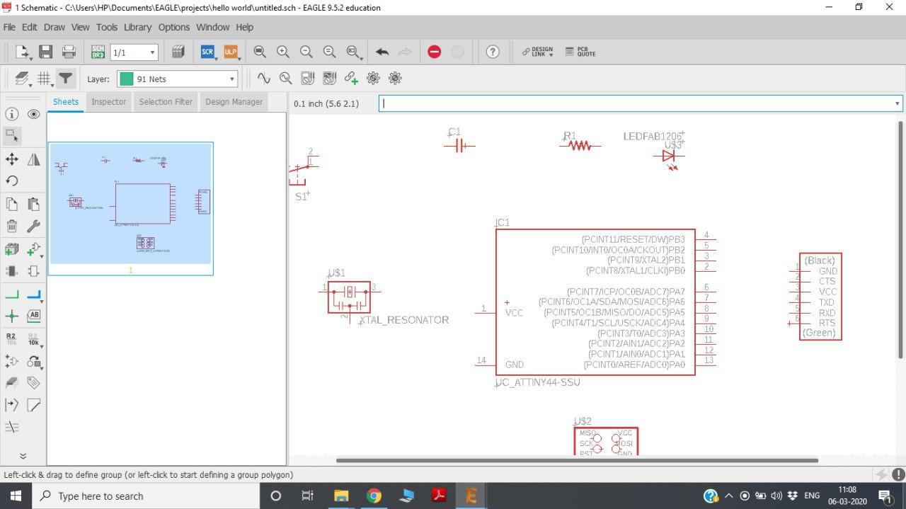
After referring the board diagrams the components are connected one by one.
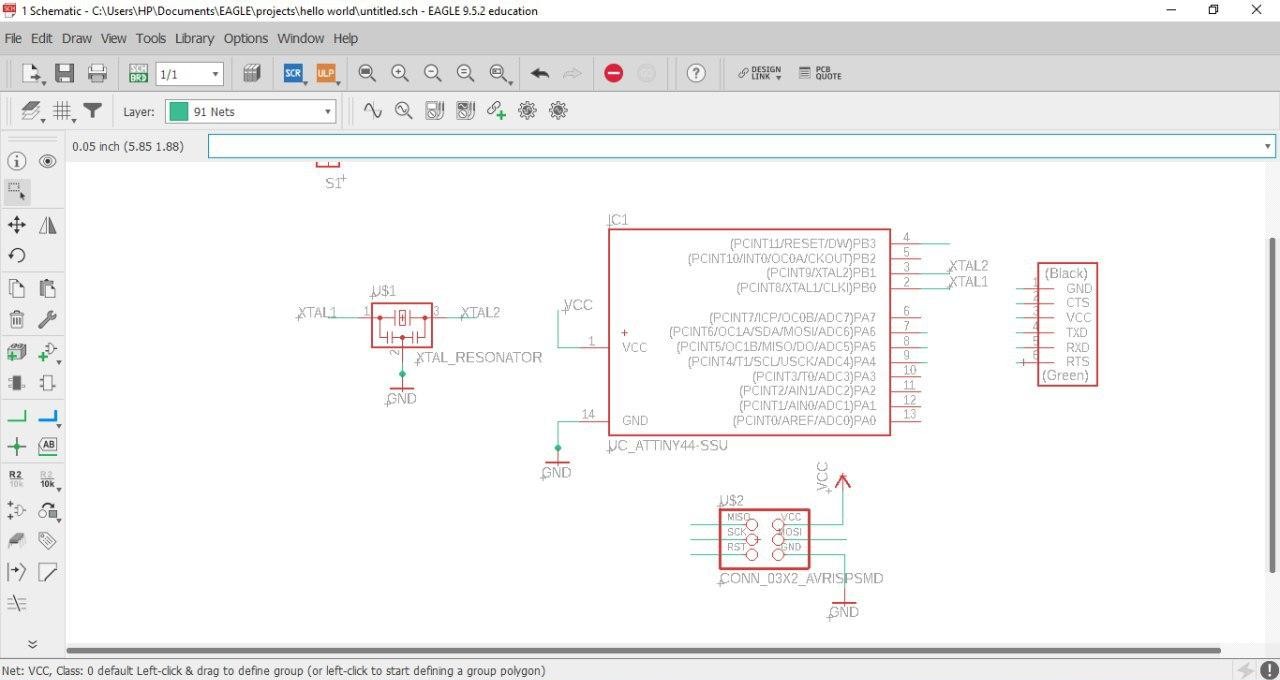
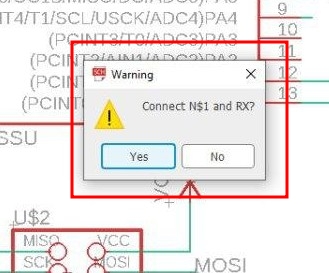
The connections are made by naming the component ends with similar names.
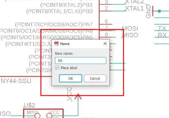
And when a window prompts us to connect each components press OK.
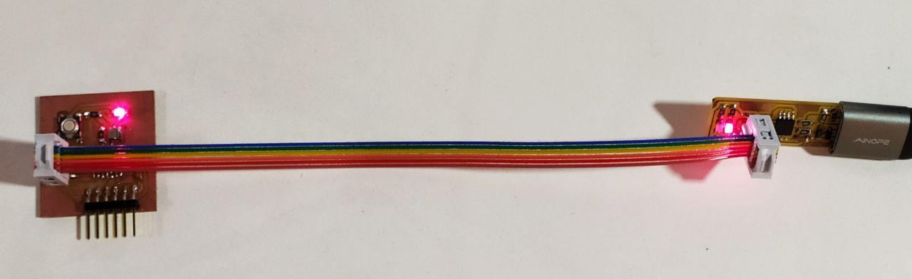
Two extra componets are added as required for our individual assignment. I placed an LED and a switch. Both Led and switch needs to be accompanied by a resistor.
One end of the switch is connected to VCC and one end to a resistor and resistor is connected to ground. And one end of the switch is connected to a pin of microcontroller
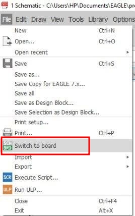
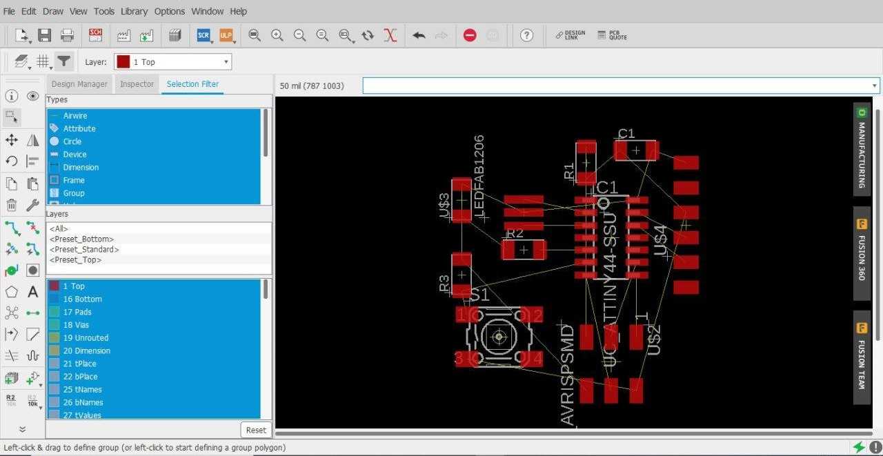
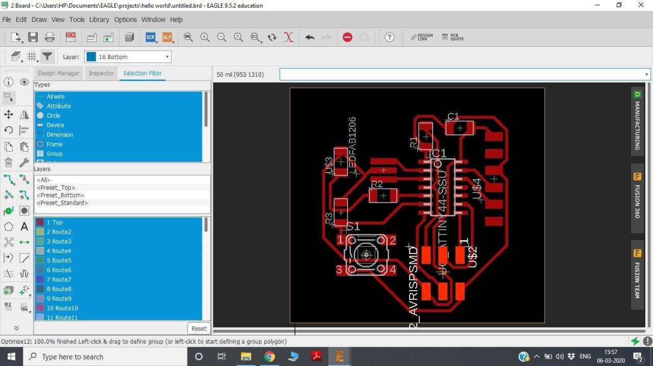
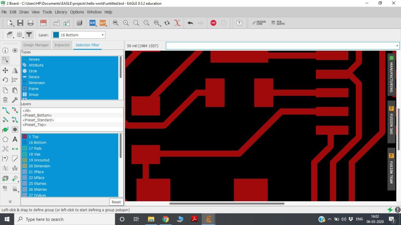
Once the schematic is completed, the schematic is transformed to a board diagram. The board diagram helps us to arrange the components and to make a proper PCB board
The components are dragged from each other with a distance so the yellow colour airwires can be clearly distinguished.
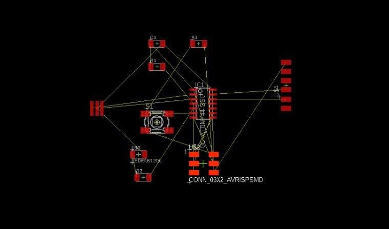
The components are arranged with minimum intersection of connections.The resonator is placed close to the microcontroller
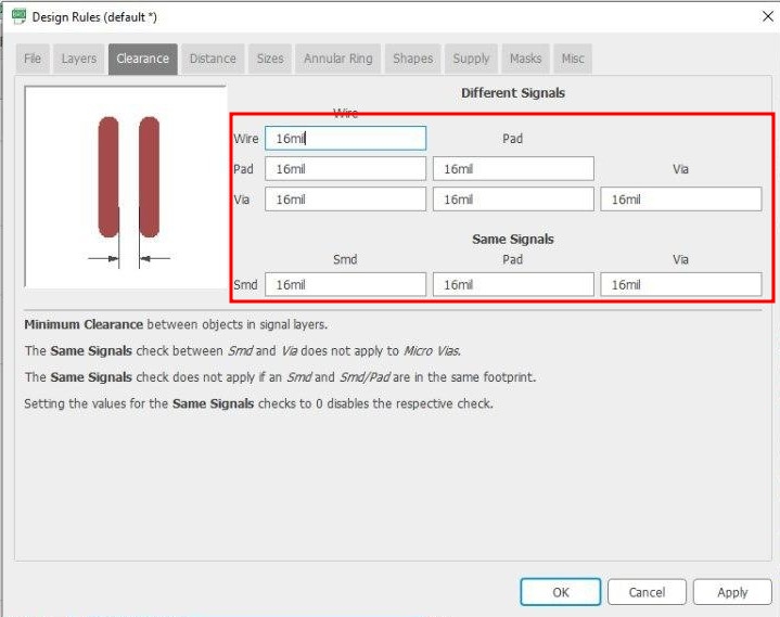
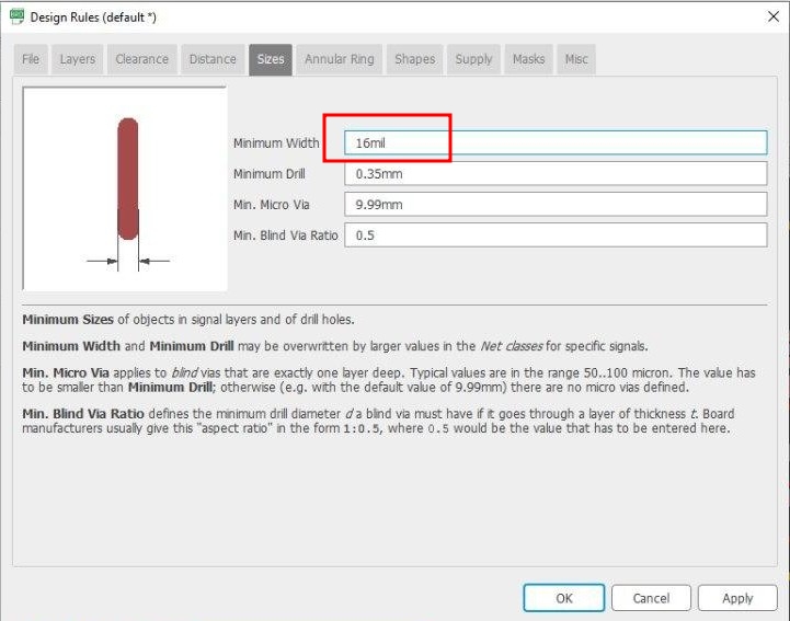
The next task is to change the design rules. The minimum clearance between each board path is changed to 16mil
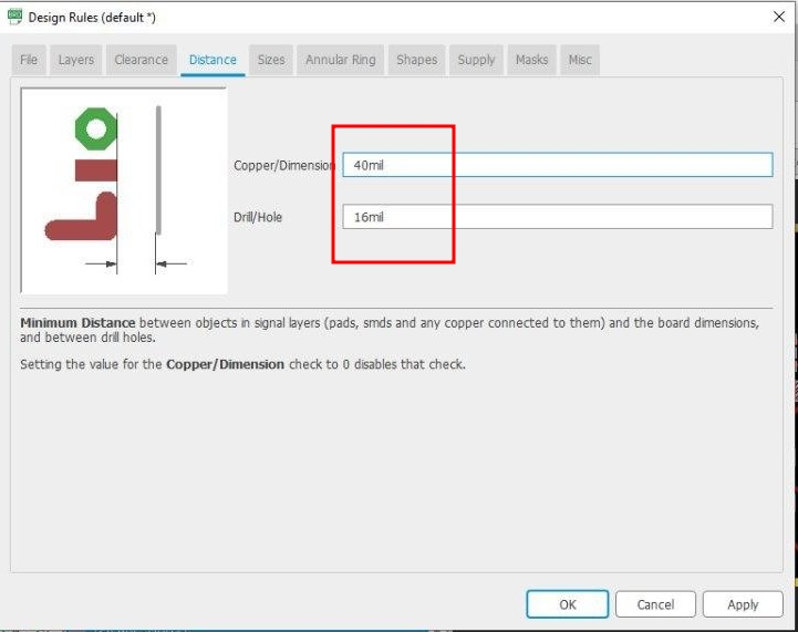
Minimum distance between objects in single layers and the board dimensions are changed.
Minimum width is changed to 16mil.
After changing the design rules. Auto routing is done to see how the pathway between different components develop.Since there is only one layer the top layer is kept auto.
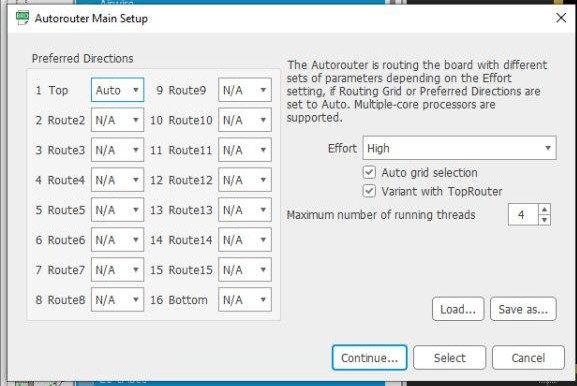
There are several possible variables in auto routing and the most efficent one which shows above 90 percent completion is selected.
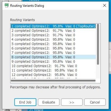
Fist autorouting had one airwire and after manuel manipulations. The circuit is complete.
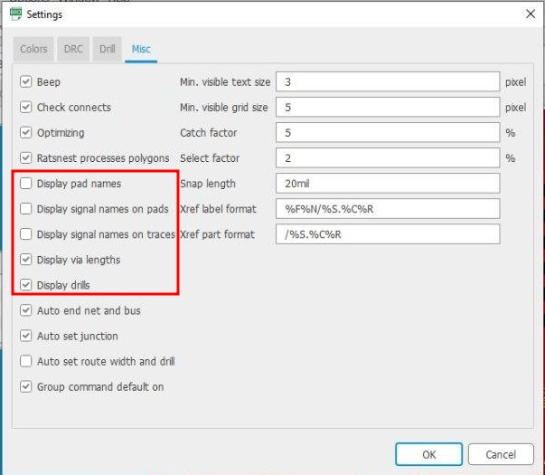
Next process is exporting this board for PCB milling. Before that all pad wrtings should be removed.For that click options=>set and a window opens up with board parameters.
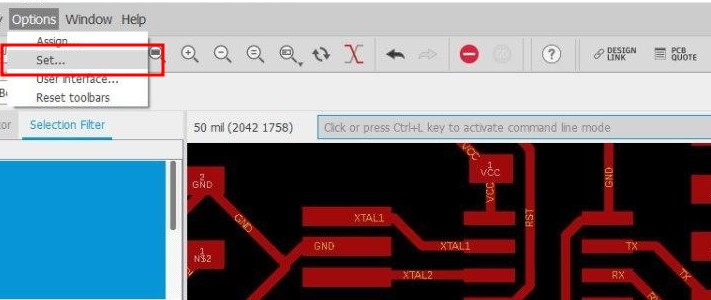
Click on misc and deselect display name options
And also select layers options and select only the parameters required for export image.
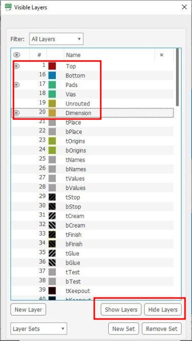
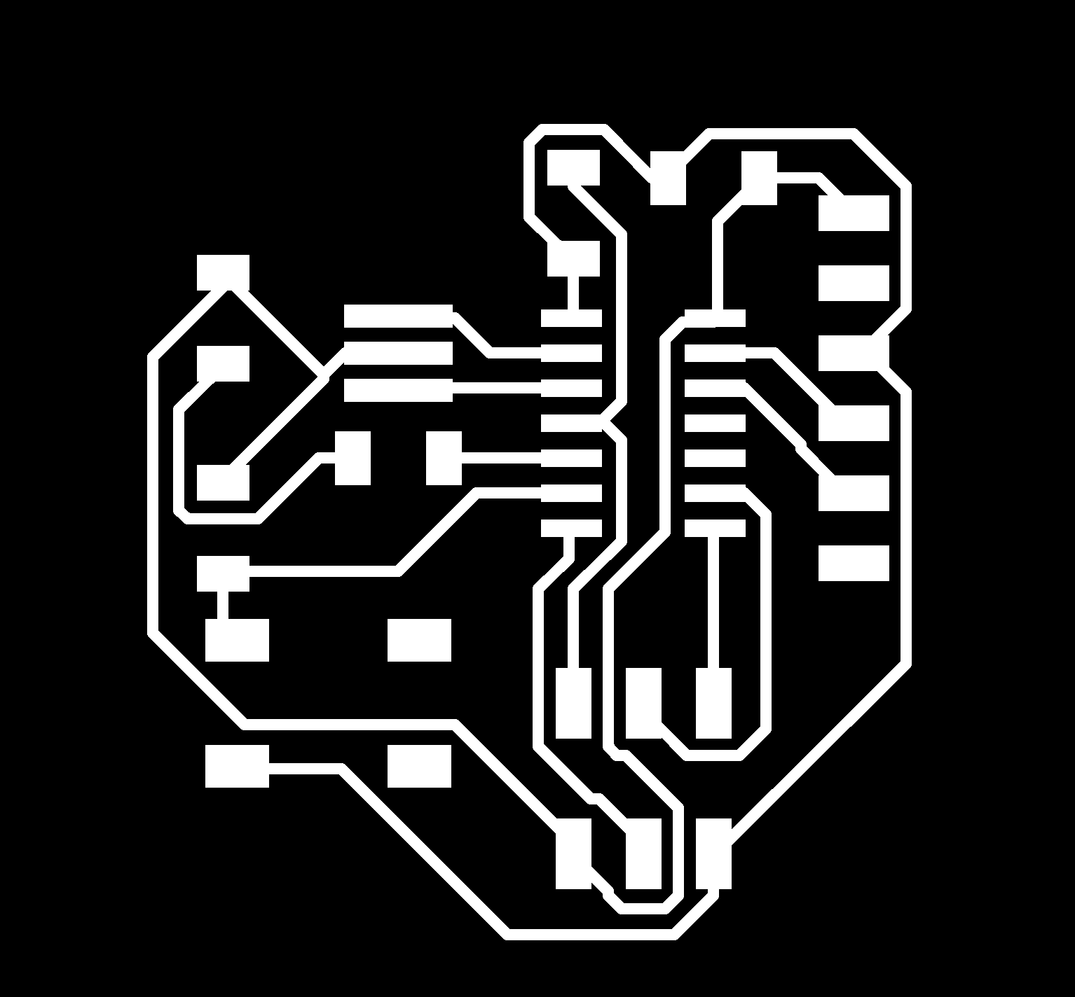
It can be seen that all writings are removed.
Next important step is to export the image.
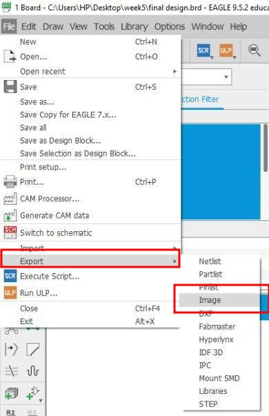
The image is exported as a monochromatic image. The pixel value is changed to 1000 dpi
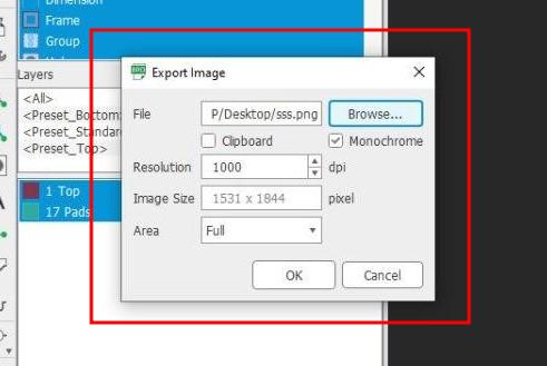
Both the trace and the boundaries are exported seperately.I later realized that for the boundary it should be kept inside as white and the boundary as black.But while milling since i left enough space between the trace and boundary, I didnt face much problem.

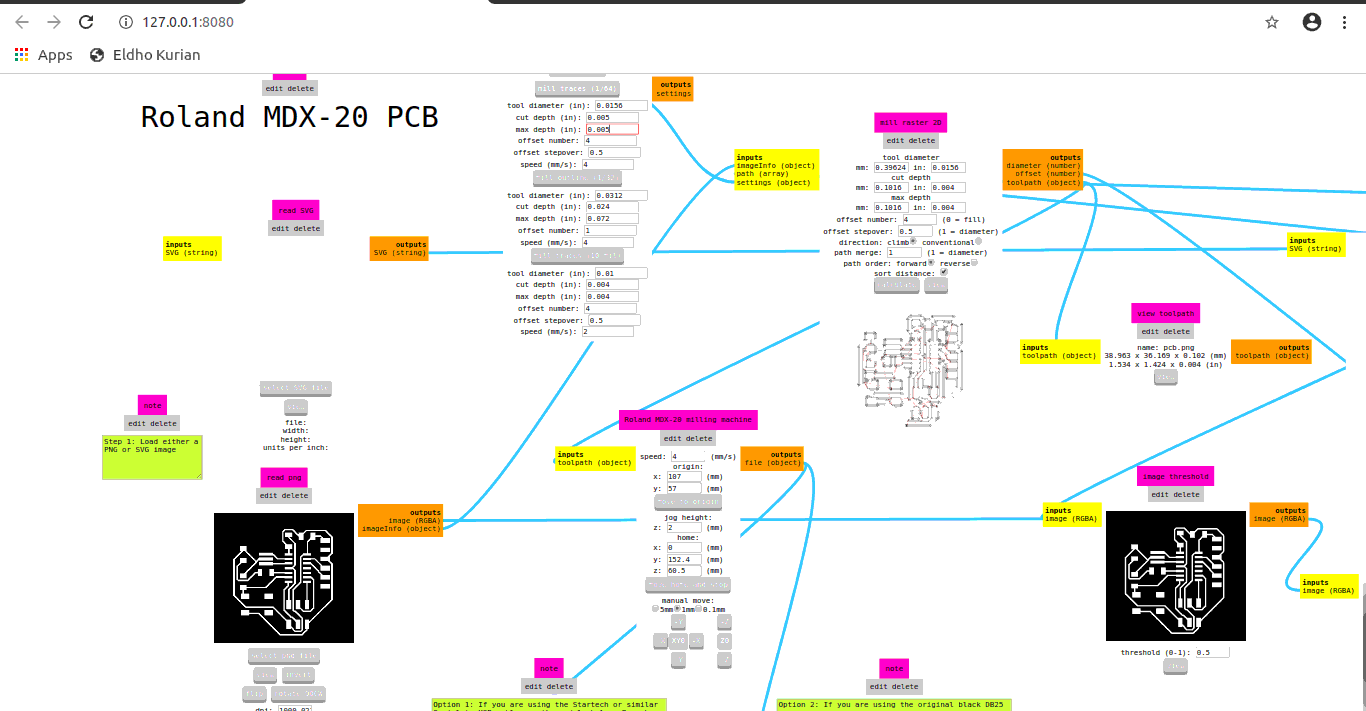
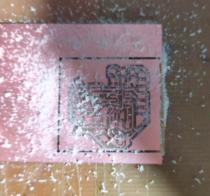
MODS programme is used as milling interface.The steps are well explained in the electronics production week.
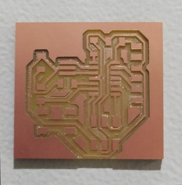
Milled PCB board
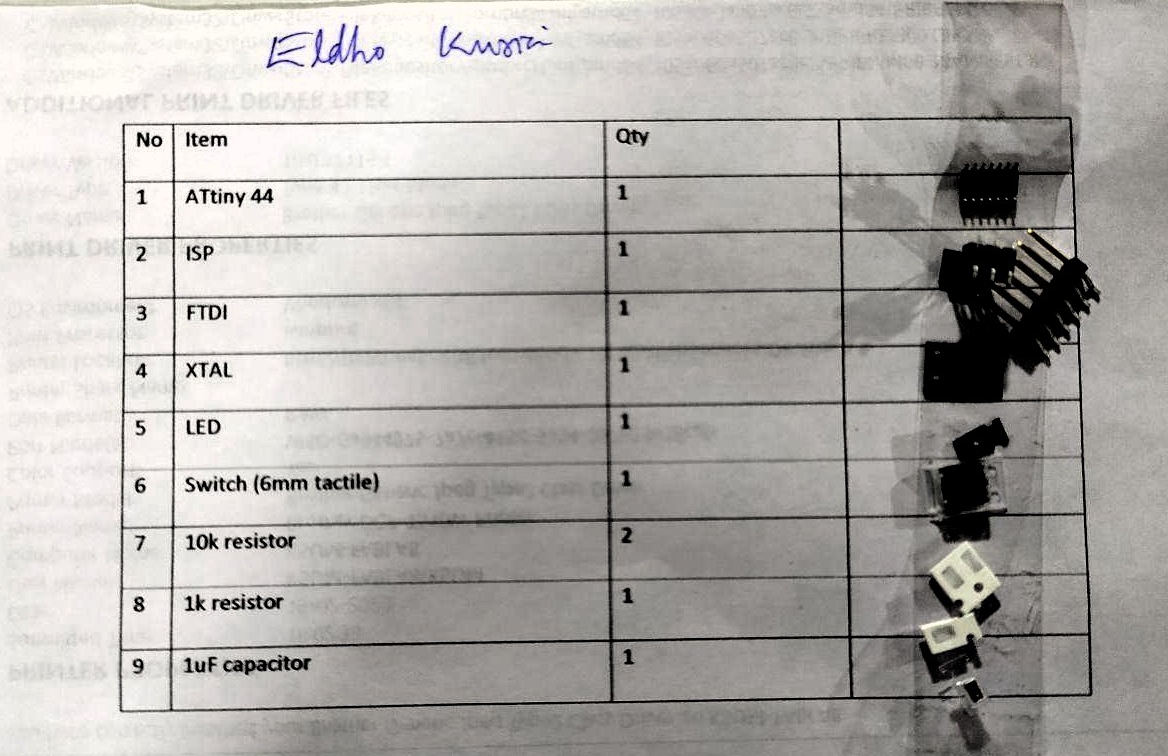
Several Components are used for soldering
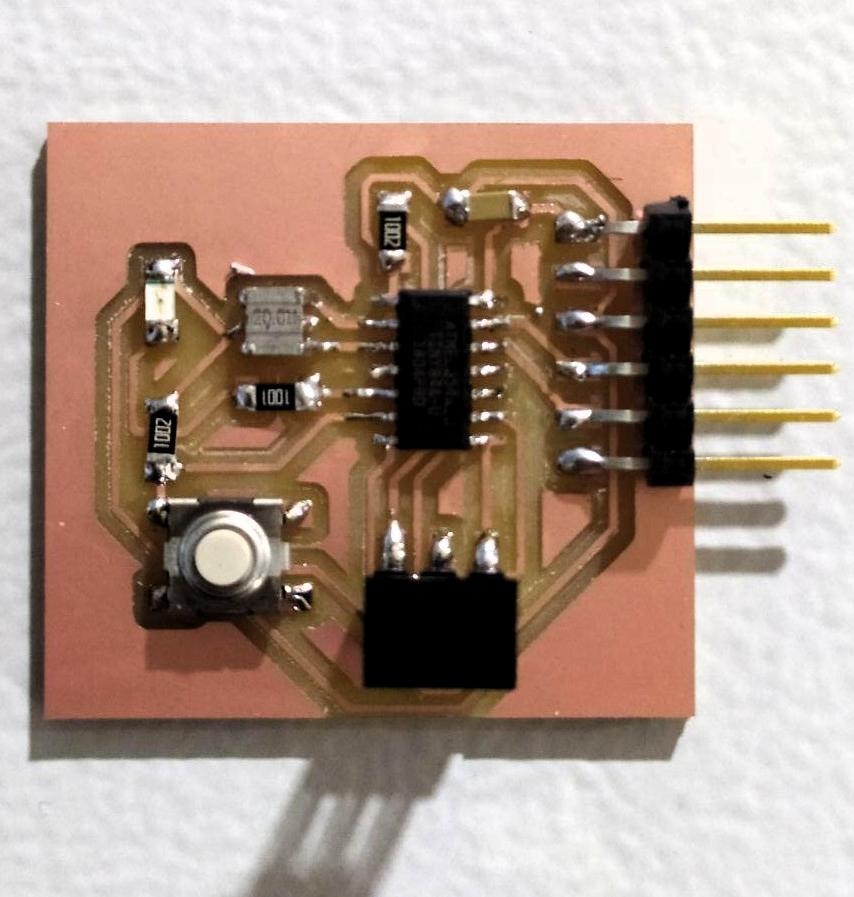
Later on the hello echo board is programmed using USB tiny to blink the led with delay of 1 second.
All design files
This week I understood the complication in designing a PCB board.In embedded week the programming part of the board will be explained clearly.
Group assignment
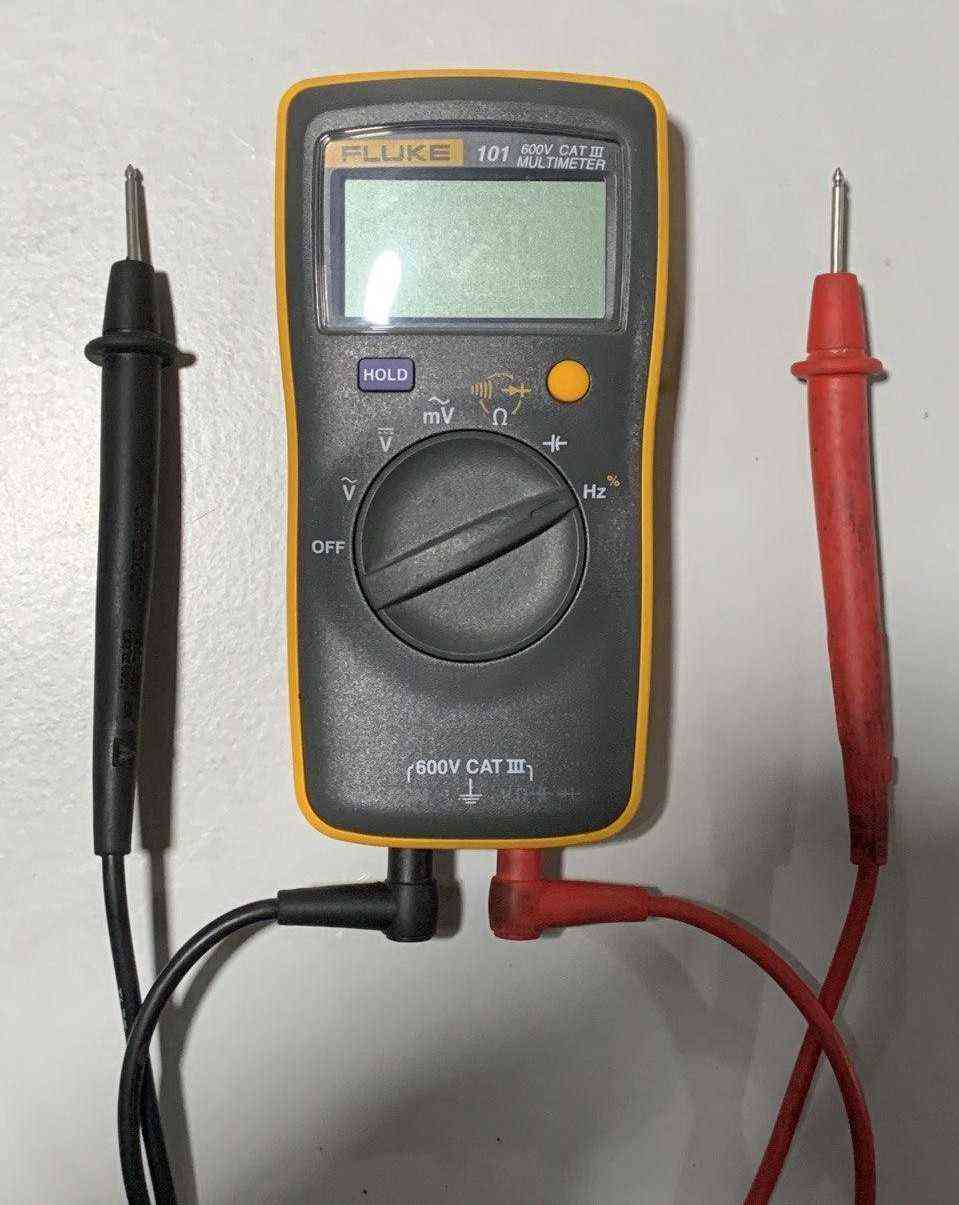
Fluke 101 Pocket Digital Multimeter
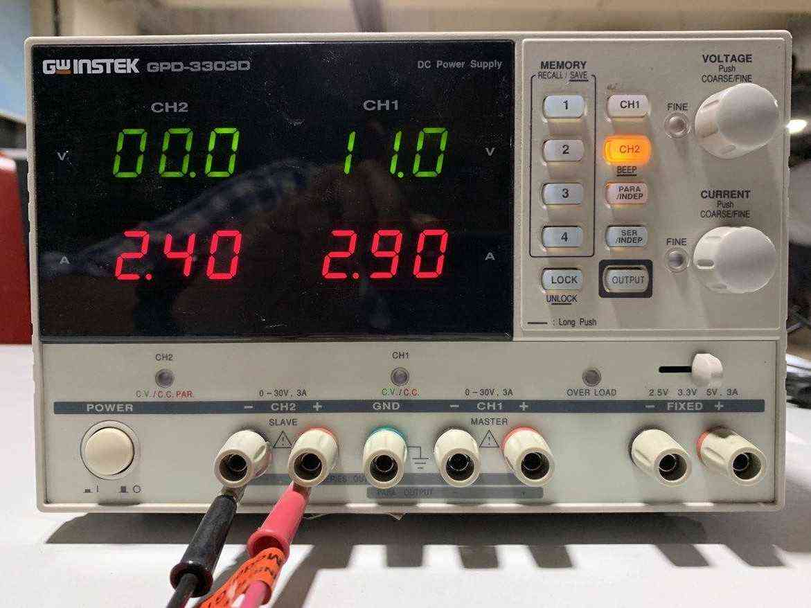
Instek GPD-3303D
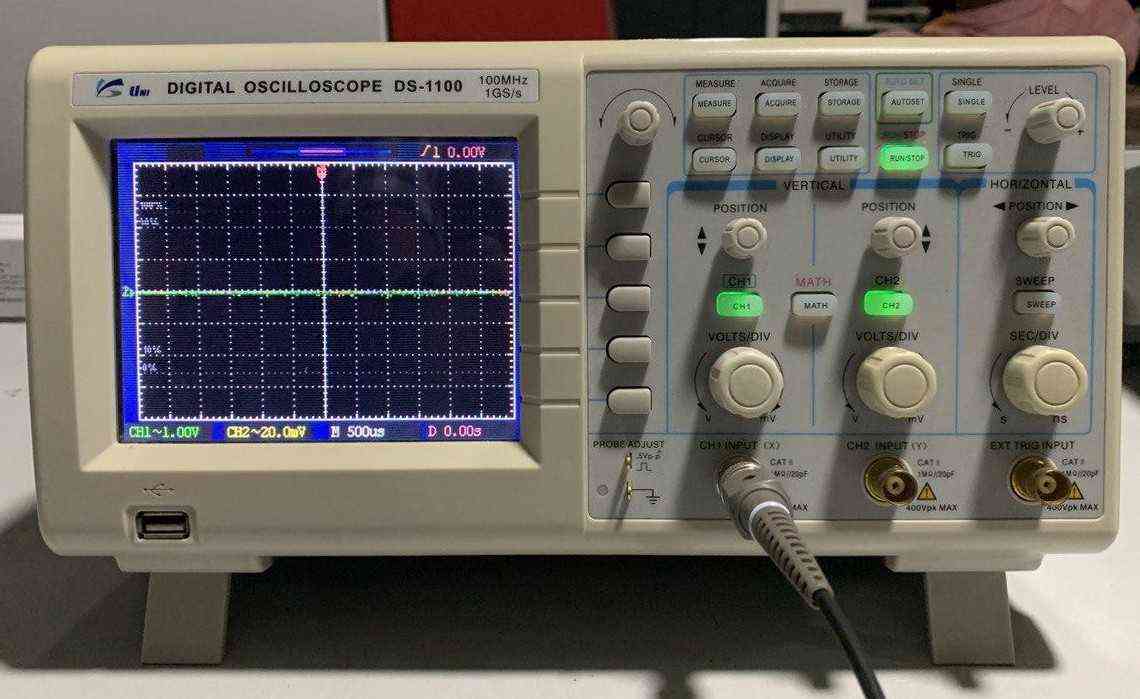
UniSource DS-1100 100 MHz, 2 Ch, Digital Storage Oscilloscope
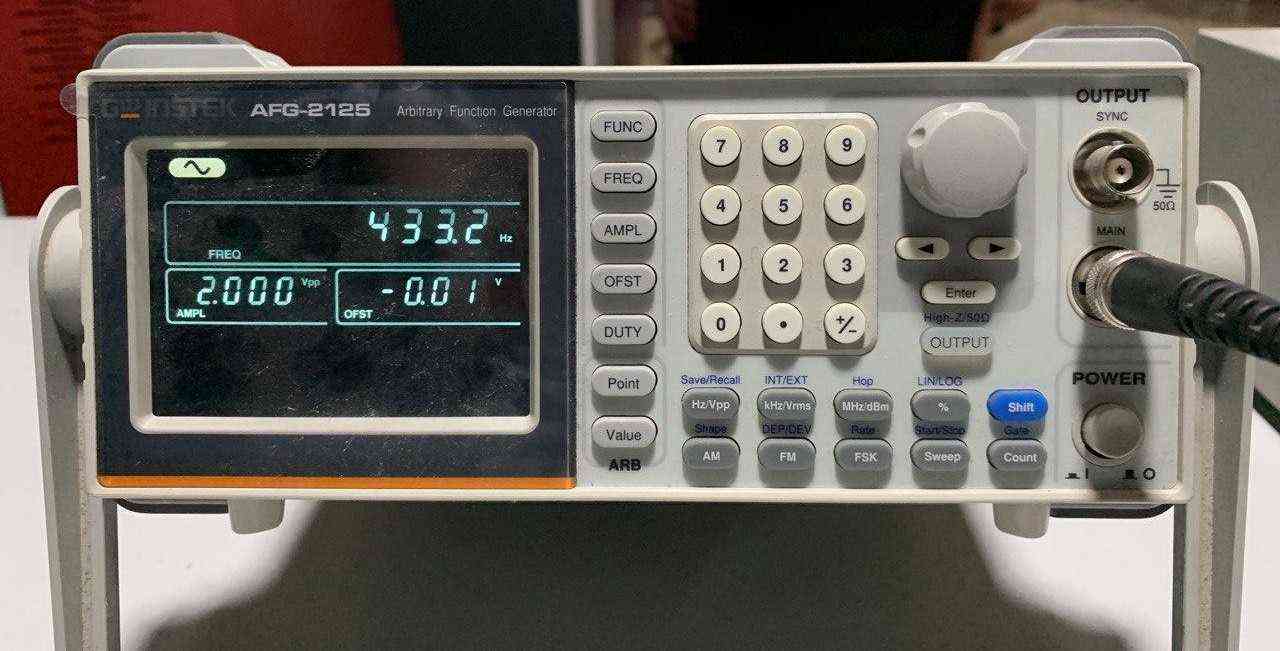
AFG-2100/2000 Series Arbitrary Function Generator