What has not been done
or what went wrong...
During my design I walked into some dead allyes. Just to remind myself that I have done them, but to prevent that they clutter my main project page, I list them here.
Research and tips
- Quentin Bolsee has a tip on getting a clock in my project. That would eliminate the need for an external webserver and wifi!
- An instructable with the RTC
- Tips for Writing Bulletproof Real-Time Clock Control Code(pdf)
- CharliePlexing made easy
- Nadiehs' charlieplexing adventures
- Charlieplexing tips
External advice:
After a talk on FA-global time I had some more ideas. Mostly to make it simpler.
- Engrave the icons of the different columns on there: not sure: I might want to change the function later... and adding a new vinyl sticker is easier.
- Make it thinner: use vinyl, instead of Acrylic; good idea. But do not have translucent vinyl, Maybe Loes can help me with this; but in the end I do not like the cheaper appearance it will give to the clock.
Things I tried but reverted on:
Split up power and TX/RX.
- I want to power the board over USB, so I need to add a micro USB port.
- I add two pins for the Tx and Rx that point up straight to be able to program the board. (I don't want them to point of the side of the board)
- I try to have the program/run switch on the edge and hope that I can make a hole on the side of my design so I can flick that switch when it is mounted.
Because I seperated the power and program functions I need to look for a part that serves my needs. It should:
- Point upwards
- Be Pin Through Hole (Henk warned me rightly that an SMD pin of this size will become fragile)
- Have at least three pins. First I thought that only Tx and Rx would be needed, but there should be common ground, so an extra GND pin is needed.
The main issue is that there is no connector in the standard FabLab Library of Kicad. So I'll have to draw it myself.
This way I ended up with a board that has two connections: one for power and one for programming. This does not fare well with Henk and I also do not like it. I revert to FTDI connection and make it a thru-hole connection.
Also, in the regional meeting, Quentin Bolsee says I could combine it all in the USB. He and Nicolas said he really shouldn't be hard and I will then be able to program the board and power it over USB. I am not sure; this will probably mean I need to add a SAMD microcontroller to the board and that adds complexity.
According the Quentin I could:
- Use a press-breakout to program an SAMD chip
- Use his binary to put on the SAMD to turn it into a USB/serial adapter (to be received at time of writing)
- Add this SAMD to the board and connect one side to mini-USB and the other side to the ESP32
I like this idea and it adds to my desire to use as little parts as possible. But the added complexity forces me to push it to another spiral.
Making an LED test board.
My first goal is to make the LED side of the board. I was having doubts on where I should put the transisters. As far as I can predict my options are:
- Next to each LED comes a transistor.
- On on side of the board I put all resistors together and then trace to the LED's.
- I put the resistors on the other side of the board, with the ESP.
The last option does not seem necessary as the resistors are so small that they can easily fit next to the LED's. If I should put all R's together or each next to it's own LED is somethign I will resolve when making the traces in KiCad.
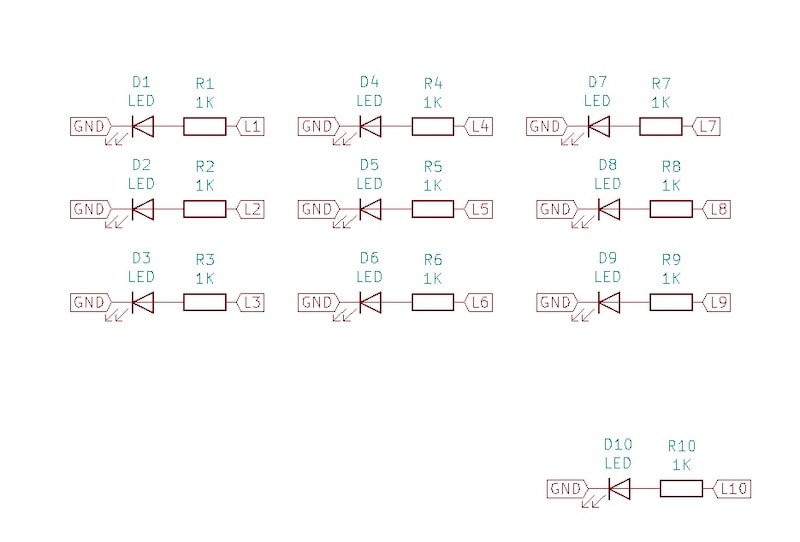
I placed the LED's in a schema
And then did some routing
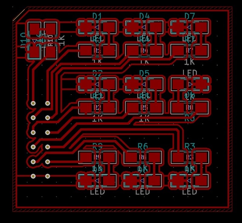
exported the lot

And then when you are just about ready to print...
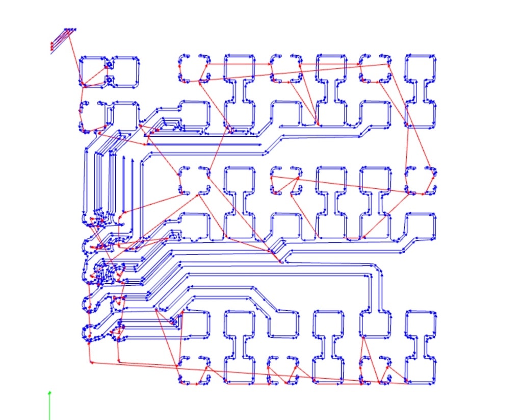
you realise that there is no even vertical distribution of LED's... So I will need to do this again... but, as most of the practice has now already been done. I think I will no longer make a test board, but make a bold attempt to make my final board. I mean, why not? what could possibly go wrong?!