| This week | |
|---|---|
| Presentation electronics design | http://academy.cba.mit.edu/classes/electronics_design/index.html |
| video of the review (3d scanning and printing) | http://archive.fabacademy.org/archives/2018/lectures/fab-20180228.html |
| video of the lecture | http://archive.fabacademy.org/archives/2018/lectures/fab-20180228.html |
| video of the recitation on bio academy (Kate Adamala, David Kong, Jean-Michel Molenaar, Megan Palmer) | http://fab.academany.org/2018/lectures/fab-20180305.html |
| Assignment | Used software | Files/Downloads/links |
|---|---|---|
| Hello World | Kicad | helloworld-0.2.zip |
| Traces file | kicad1-F.Cu_final.png | |
| Outline file | kicad1-Margin_final.png |
The week in an overview:
Last week was spend in Paris, because of a short holiday (my 3 kids had their spring holidays from school). At wednesday I visited the Sorbonne University Fablab to follow the local review. Handy, because the fabacademys at amsterdam and paris are connected for the review by mentor Emma Pareschi. It was nice to meet Vincent, Adel and Ben and see the Sorbonne Fablab in full action. Thierry was that day connected from Amsterdam, looked like a kind of exchange :)
Anyway! That week was a week well spend with family and visits to the Eiffel Tower, Arc de Triomphe, Rodin Museum, Museum National d’Histoire Naturelle and some other Paris hotspots. I didn’t do a lot for the fabacademy… I had some time on monday and thuesday and managed to review big parts of the local lecture by Emma on video (thanks Johanna!).
Kicad
For a longer time i wanted to learn kicad, so finally it was time to dig into it. It were 2 exciting days :)
I’m gonna write down the learning proces. For me that normally is something like the following schema:
- try, and figure out the basics
- RTFM or google answers that popped up
- watch tutorial
- try again with the learned basics, both from the first try’s, google and watching tutorials
- once done, i redo the whole project and document
It worked out pretty well!
The video tutorial:
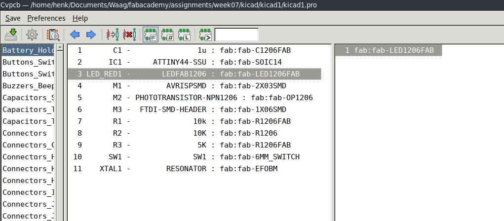
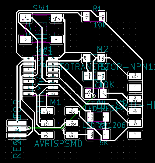
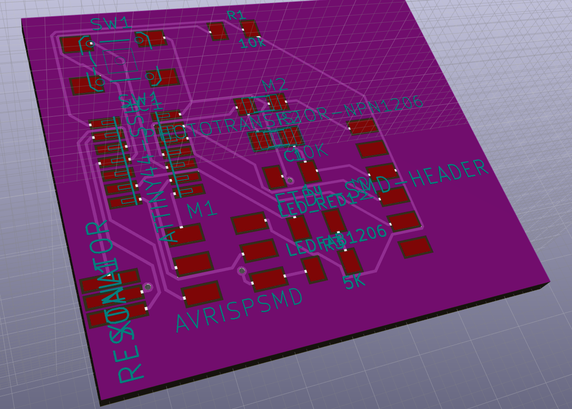
First thing to do is make the eeschema. Find and place all components was a journey, a long one, but once i understood how it works, it became a more or less easy job. I used the fab.lib and fab.mod from the fabacademy site. Emma suggested to include a few more components, here is the complete list of components:
List of components on my Echo Hello board:
6-pin header
Microcontroller ATtiny44A
FTDI header
20MHz resonator
2x Resistor (10k)
Resistor (value unknown till I calculate for the LED)
Button (6mm switch)
LED (red)
Resonator (220-MHz)
Phototransistor
Capacitor (1uF)
Ground
VCC
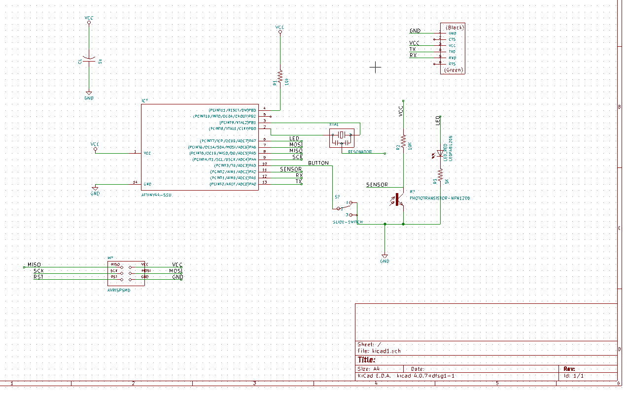
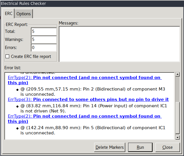
Once done i used the Electronical Rules Checker. I had to name a few legs to finish the electronical schema.
The next step is to associate the footprints with the components. That is done with the cvpcb were suggestions come up (and you have to comfirm) and when needed, you need to find the right foodprint. I didn’t had to edit any undocumented footprint.
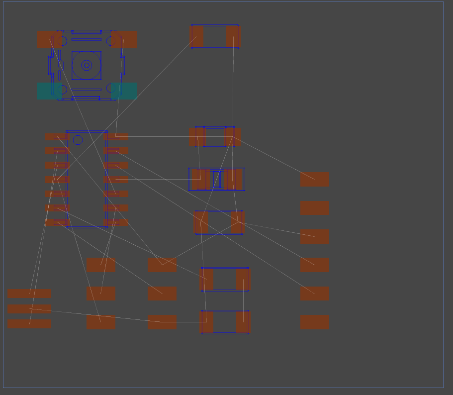
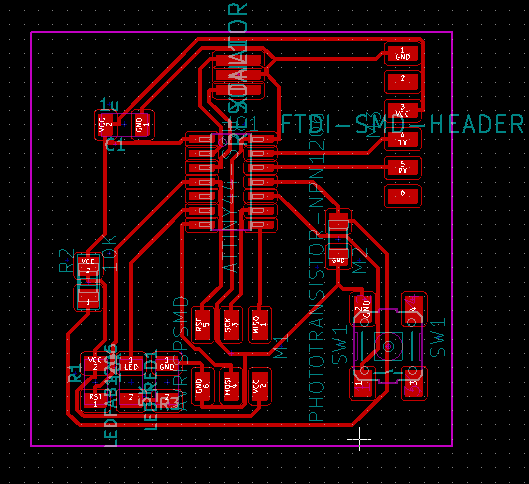
Now you have to open the PCB layout editor. It opens up with unorganised footprints from the eeschema with connections and looks like this:
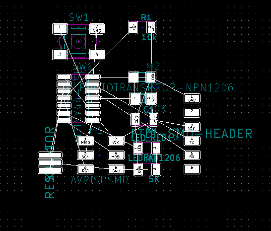
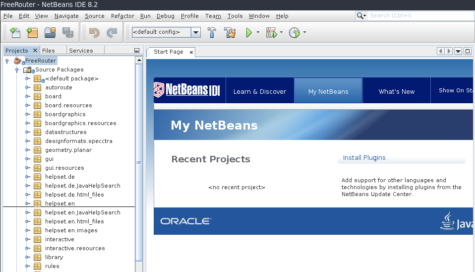
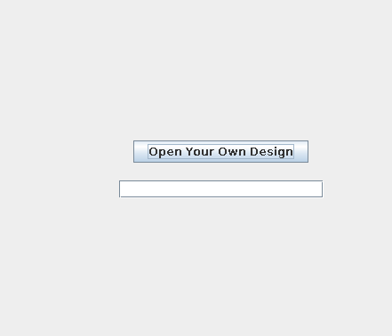
I ordered the components a bit and place a outline of the board. Now i had to route the tracks. It’s a puzzle, nice when you have a lot of time and nerves. Since i used a rc2 of the nearly released version 5 of Kicad, i had troubles with the buildin autorouter. I found another router called [freerouter]https://github.com/nikropht/FreeRouting() and used this tutorial to install it. It’s a Java Based Printed Circuit Board Routing Software written by Alfons Wirtz, released under GPLv3.
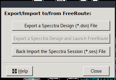
Anyway: back to Kicad! Kicad has an options to export/import to/from FreeRoute. Once you have a organized piece ready in the PCB layout editor, you can export it in Specctra Design file. That file you can then open in FreeRouter. Here the whole process in images.
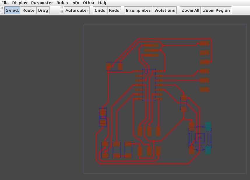
FreeRouter
import a file in freerouter
this it the exported unrouted layout from kicad opened in FreeRouter
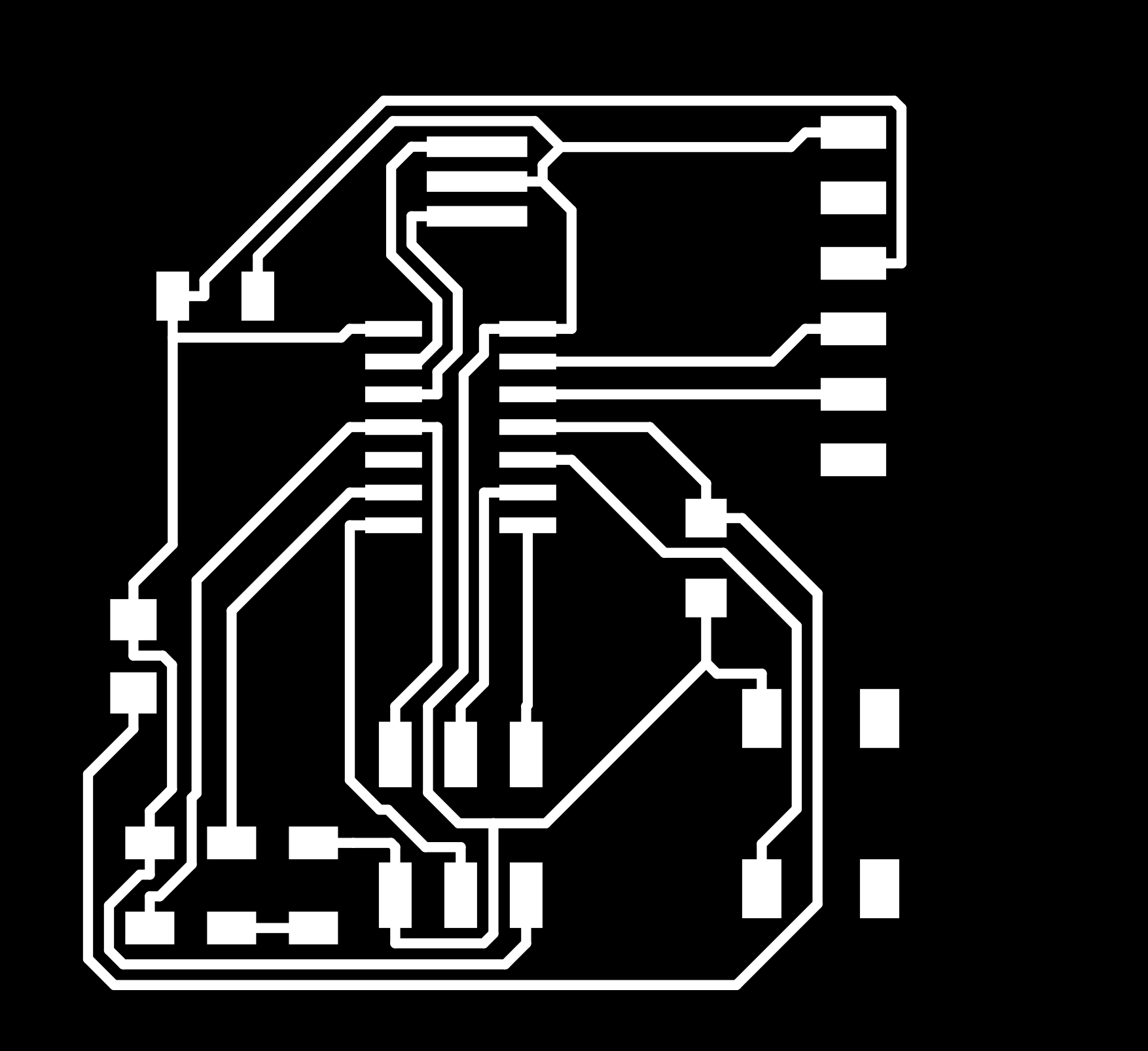
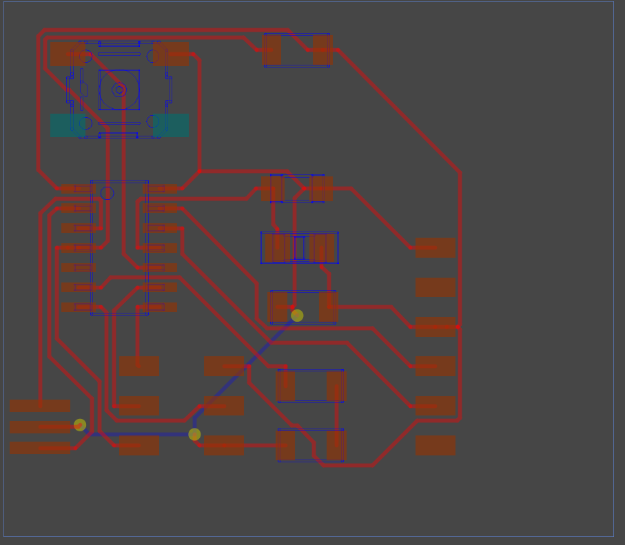
With some component reshuffling the autorouter option of FreeRouting produced this beauty.
You then save the file and import it back again in Kicad.
A nice extra in Kicad is that you can then view your result in a buildin 3d viewer.
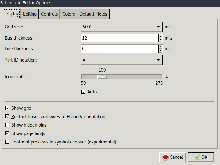
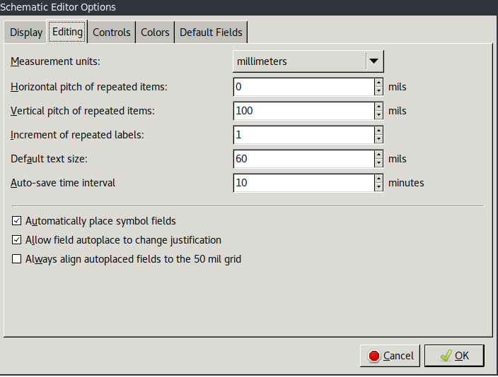
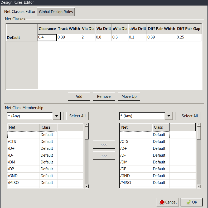
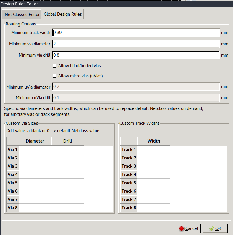
Now i’m stuck into something i forgot, or better, what i should have taken care of in an earlier stage. Namely the desginrules! So i went back to the eeschema and implemented the design rules we figured out during the electronic production week. Now i know that the traces can be milled on the modela. See here the setting from the schematic editor and the design rules editor:
export/import to FreeRouter again. Nice!
Import the result back into Kicad
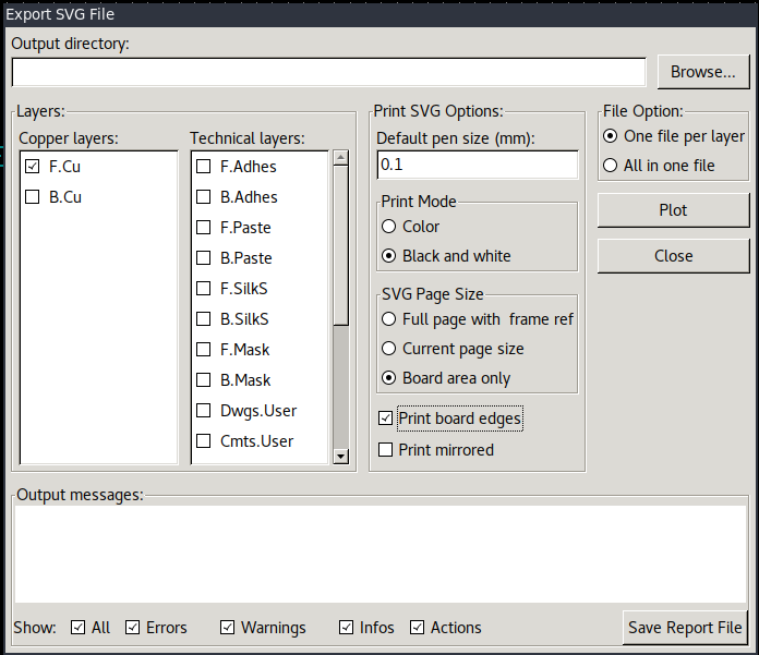
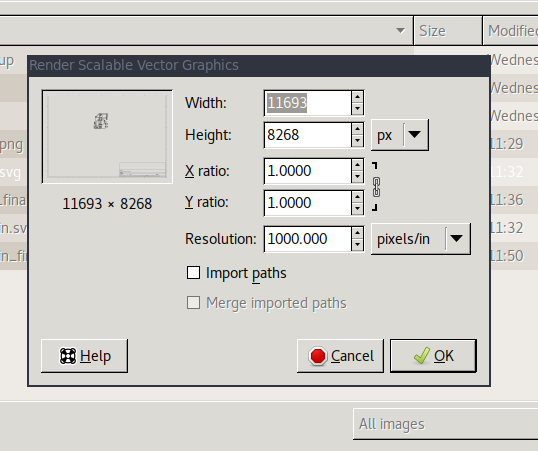
Kicad doesn’t have an option to export to a png file. So i exported to a svg file. See here the layers and svg export options.
Gimp
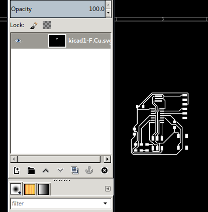
I imported the svg into gimp. In gimp i first set the resolution to 1000 pixels per inch to get a printable result.
![]()
After removing the alpha channels and inverting the colors i have a result that i can use to mill with the modela.
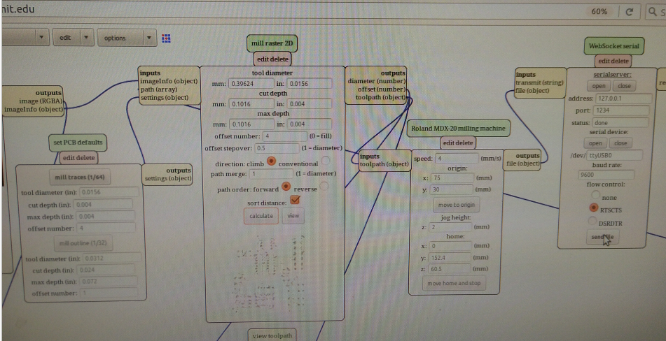
##Modela
Now the proces moves to the modela. Imported the design into fab mods, and putting the setting found during the electric production week, resulted in these setting:
The board came out very nice and the soldering of the components went without a problem.
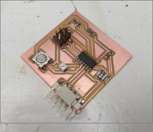
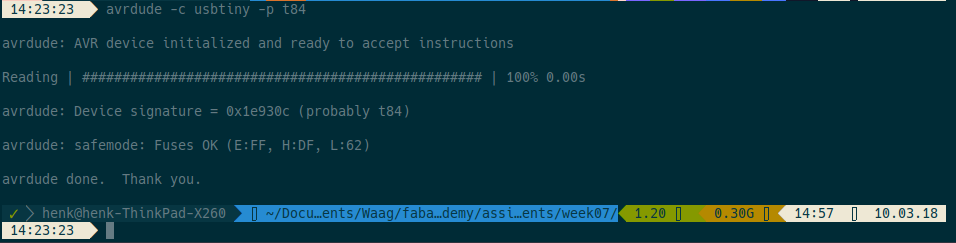
At the end it all went pretty good. Here you see how i connected the board to my FabISP produced during the electronics production week.
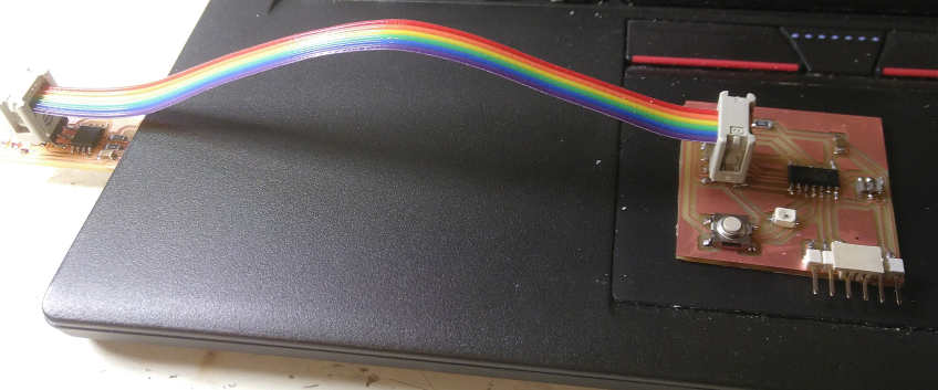
And the programming of the board went fine!