Electronics Design.
Previous Work.
After going through the system design and defining the necessary requirements for one electronic block, it is time to create the logic of the system. Parts of the system are tested in Electronics Design Week, whre the functionality of the Attiny44 microcontroller is tested, in Output Devices Week, where the functionality of the shift register is tested and in the Networking Week where the communication using infrared diode/photo transistor is tested.
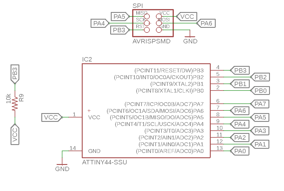
Electronics Design Week.
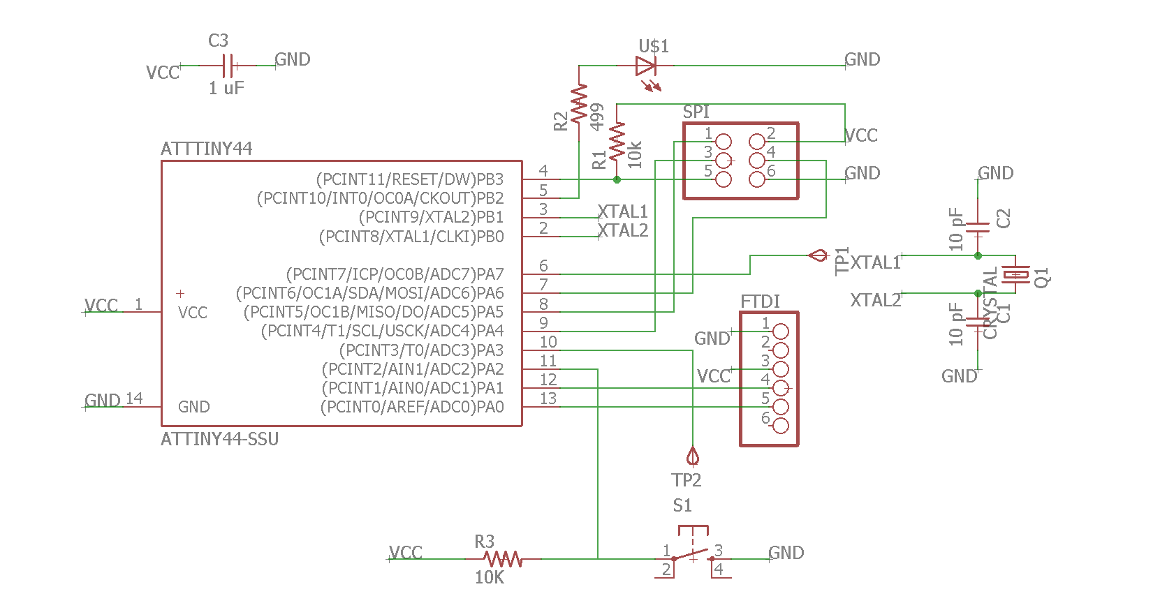
During this week the following were accomplished:
Output Devices Week.
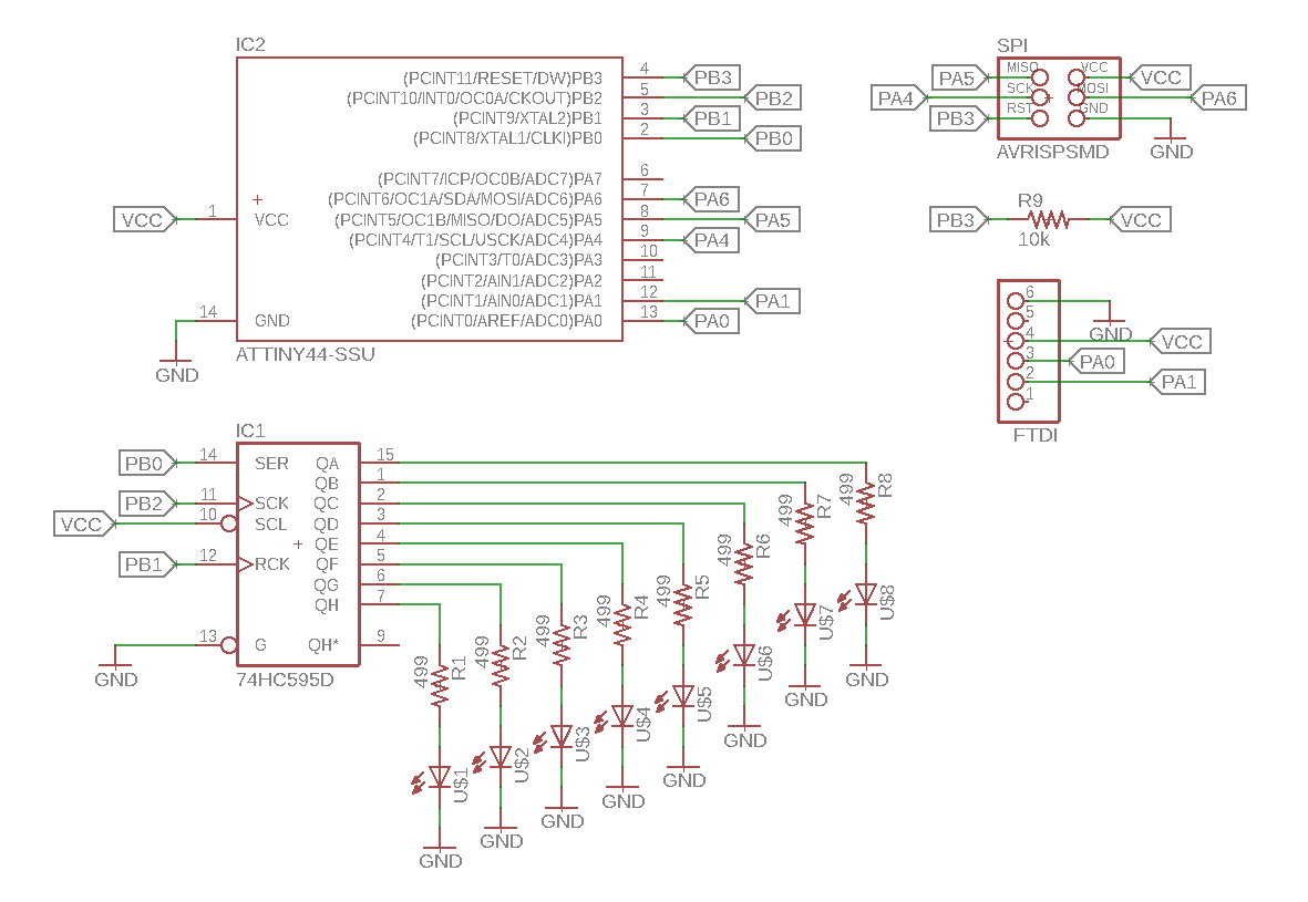
During this week the following were accomplished:
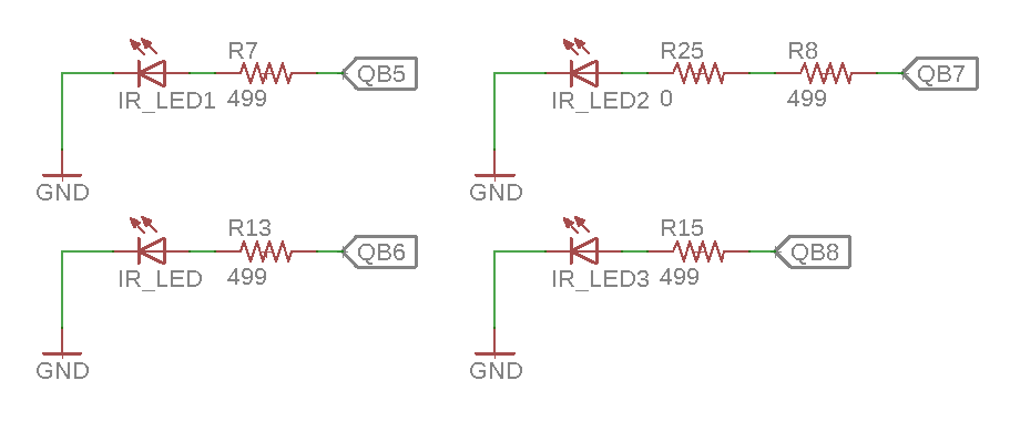
Networking Week.
During this week the following were accomplished:
Electronics Design Goals.
It's important to outline the desired goals that we want the system to achieve. Here are the goals:
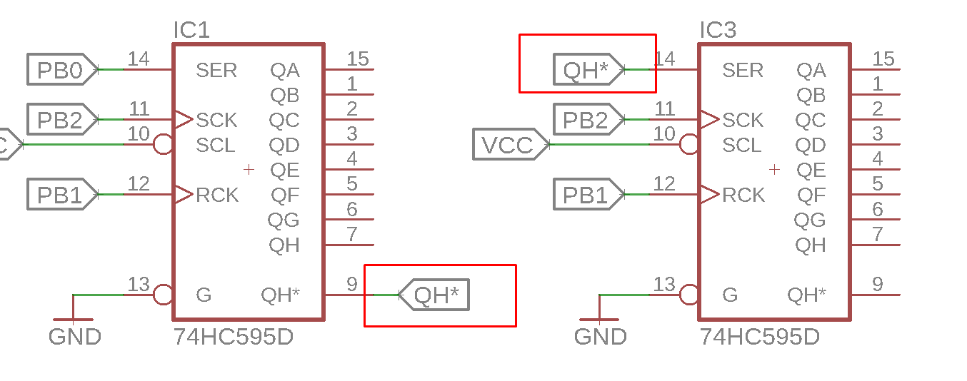
Two Shift Registers.
The advantage of having shift registers is that you can easily increase the amount of the outputs by simply wiring the shift registers using
In order to test that out, a proposed circuit is tested on the breadboard, although without using the LED outputs. To test whether the Shift Registers output a HIGH, the multimeter is used the measure the voltage across each output.
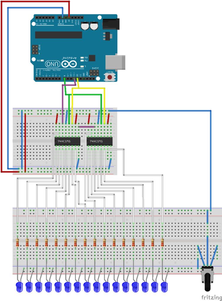
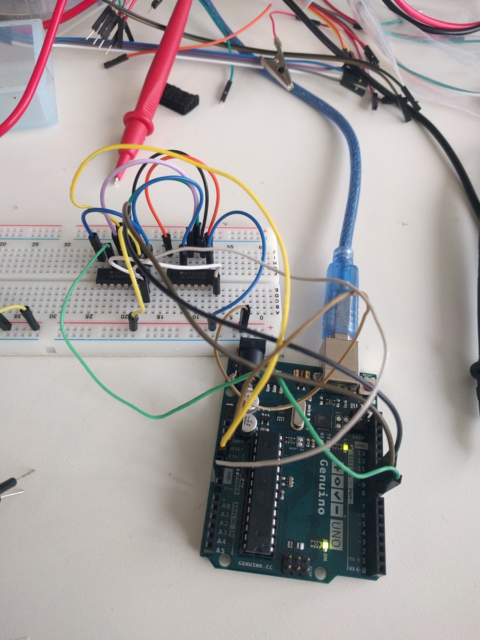
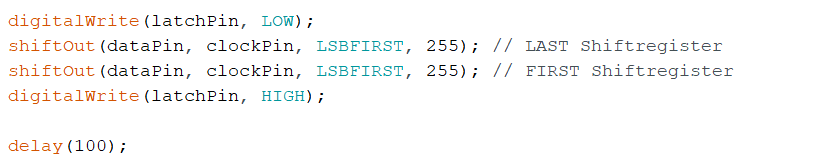
This time the code of the arduino has a slight change. To control both shift registers, two times the
As a result of this code, both shif registers were high. This was implemented in the following schematic of the system.
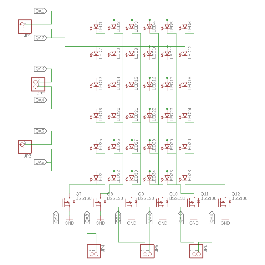
LED Matrix.
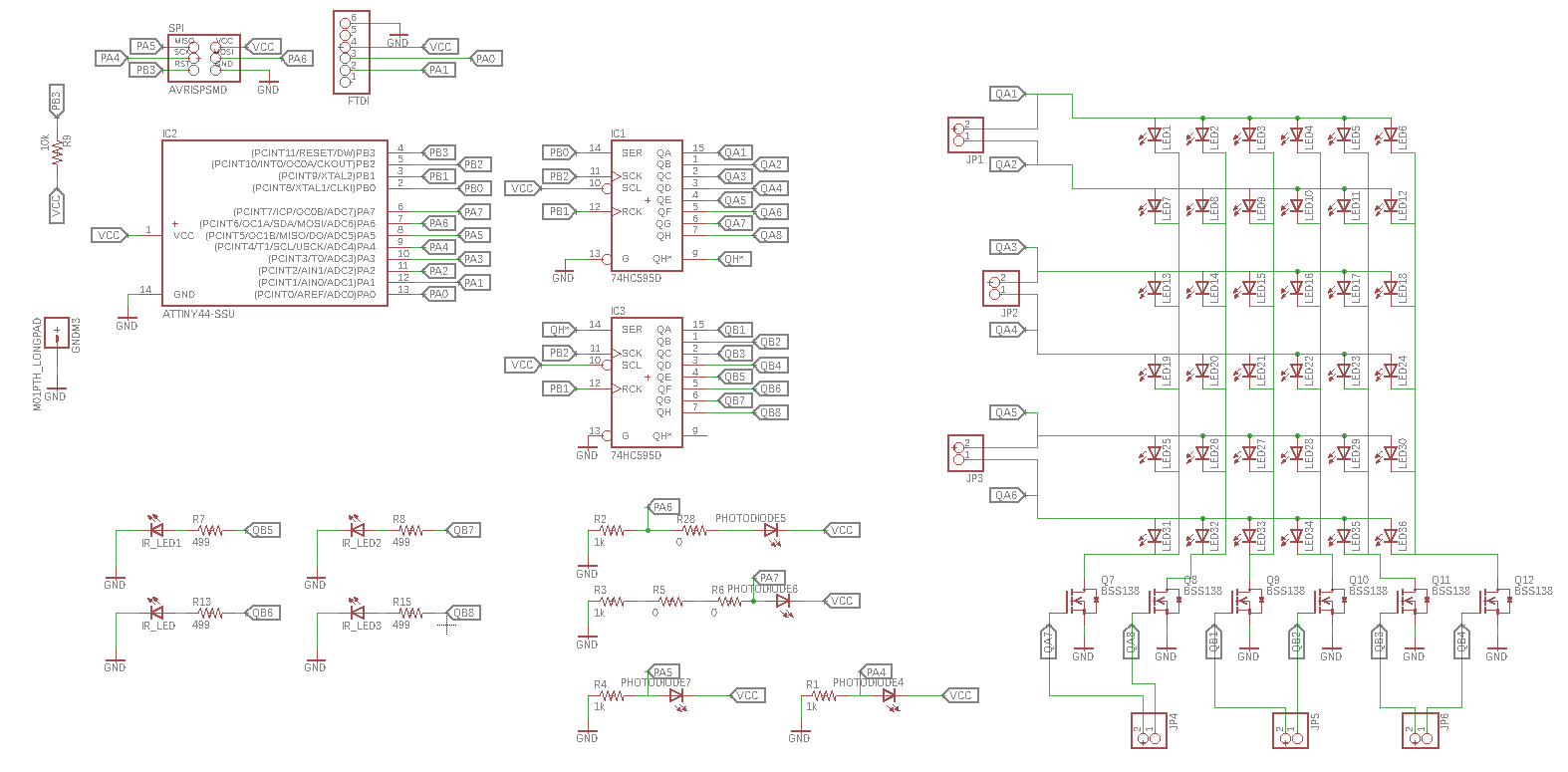
In order to achieve the control of the LED matrix, the matrix needs to be devided both into columns and rows. Having six columns and six rows already limits the outputs of the Attiny44 we can use, that's why the shift registers are implemented, by means of which we can ultimately
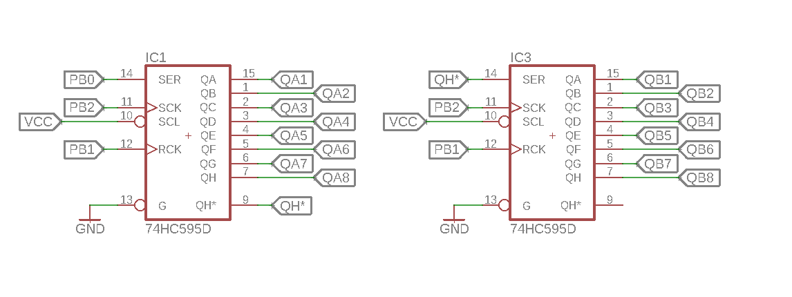
Here the first shift register controls the 6 rows and the 2 columns of the Matrix, while the last controls the last 4 columns of the matrix.
The fist solution of the circuit designed included 12 MOSFET transistor that would be actuated by the means of the shiftregister outputs. The reason for this decision was the apparent limitation of the shift register to drive a lot of current. Having 36 LEDs, each consuming about 10 mAmps, would result in 360 mAmps drive which would limit the shift register.
The MOSFET in this case would act as a switch, to which once given the necessary 1.2-2 voltage input, would conduct through the Drain and Source pins. Also the 10 ohms resistors were intended to limit the voltage drop through the LEDs.
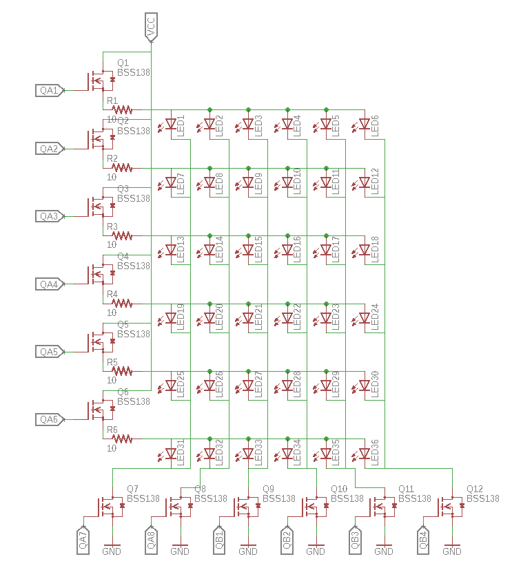
However, after testing this system, I quickly realized the MOSFET was not wired properly. By debugging the system I quickly realized that the shift register output could control one row of LEDs directly without the means of MOSFET switch. Some components were reduced, the MOSFETs for the rows and the registers.
After soldering and testing this worked perfectly fine. The bottom MOSFET enable the access to GND which allows the current flow as a result.
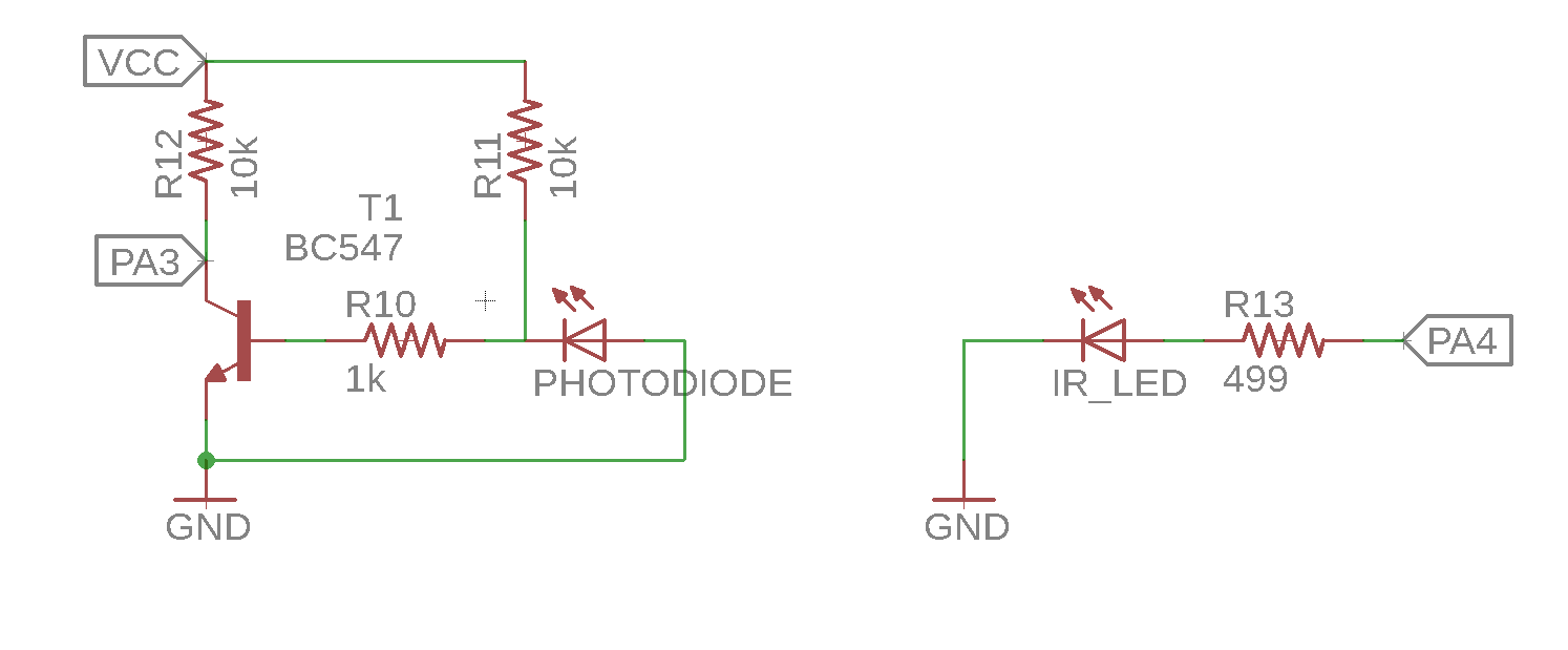
Infrared Communicating Sides.
Currently the infrared phototransistor was using up to 4 additional components to drive the ir transistor. The goal was to reduce that and the new schematic resulted.
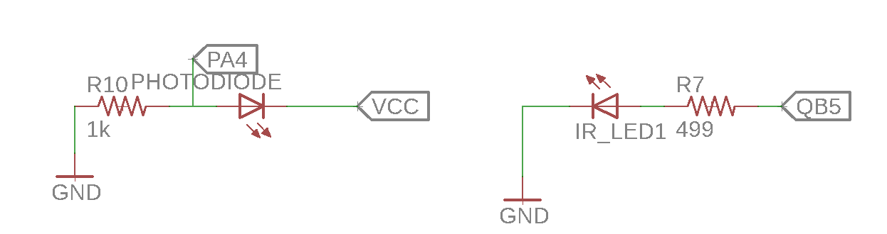
In this instance both IR received and transmitter use one resistor, with small variation in value.
This is then scaled up to 4 units per side of the cube. The 4 IR LEDs are controlled by the last four outputs of the second shift register, while the IR receivers are controlled by the 4 analog inputs of the Attiny84.
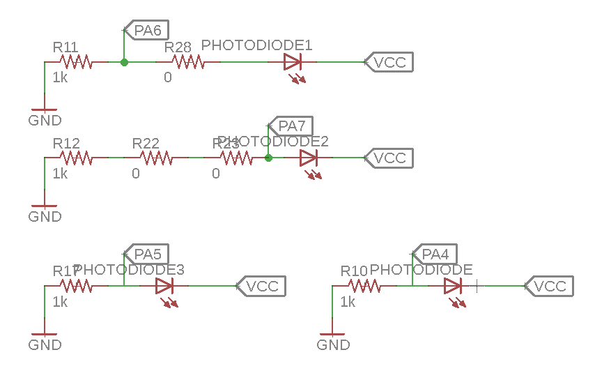
*O ohms are used only as bridges during the layout.
Final resulting schematic of the system: