Electronics Production.
Board Layout.
In order to fit all the components on a copper sheet that is 5x5 cm, keeping the goal in mind of having a relatively small cube, a heavy work of routing as well as
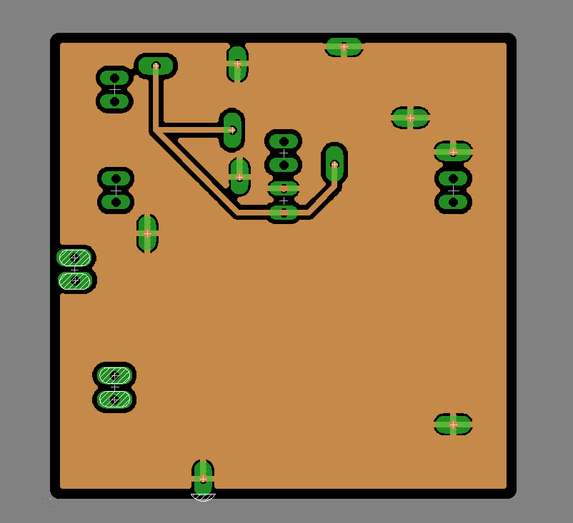
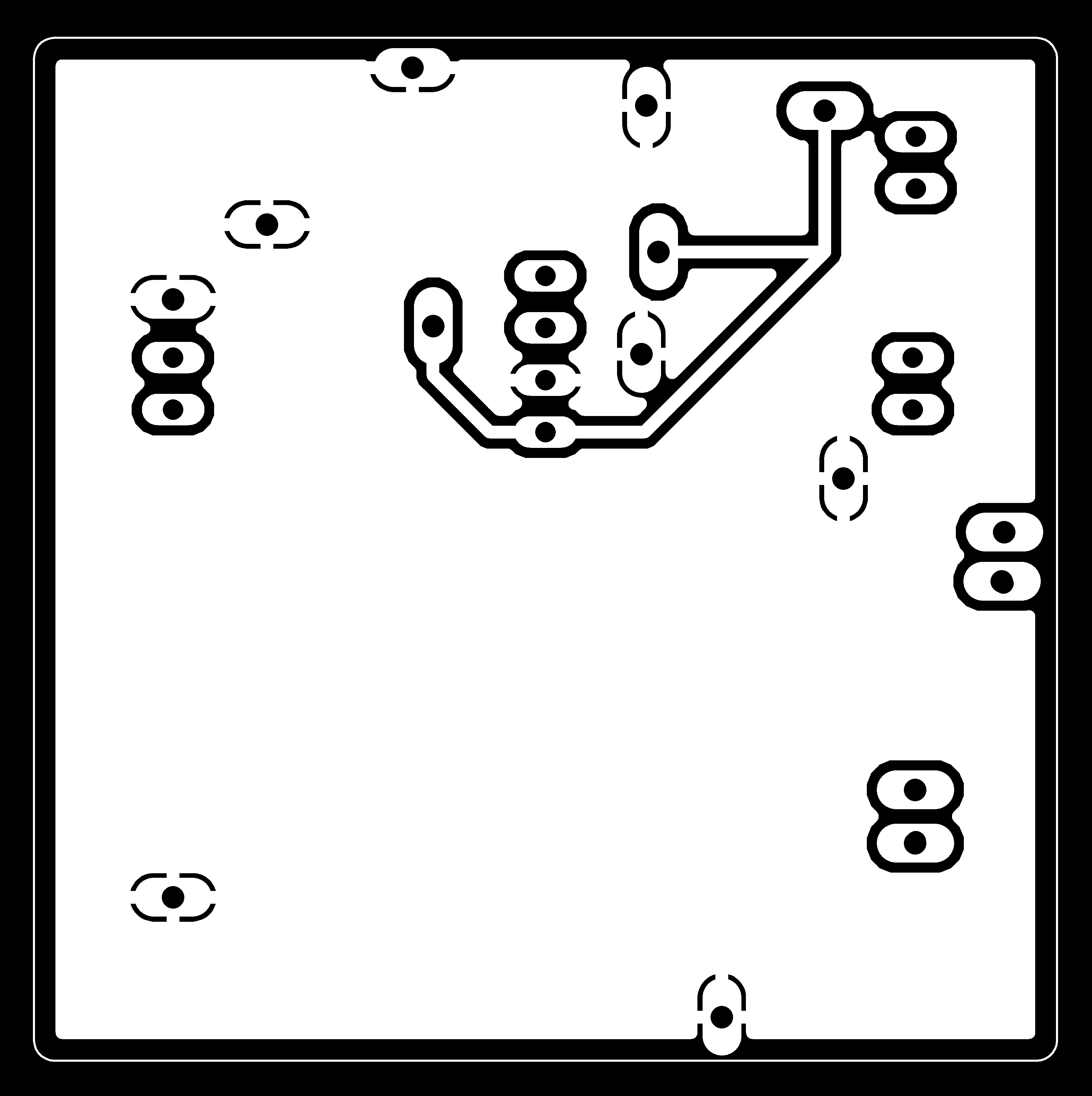
Bottom Board.
This layer is the main layer of the cube. It hosts:
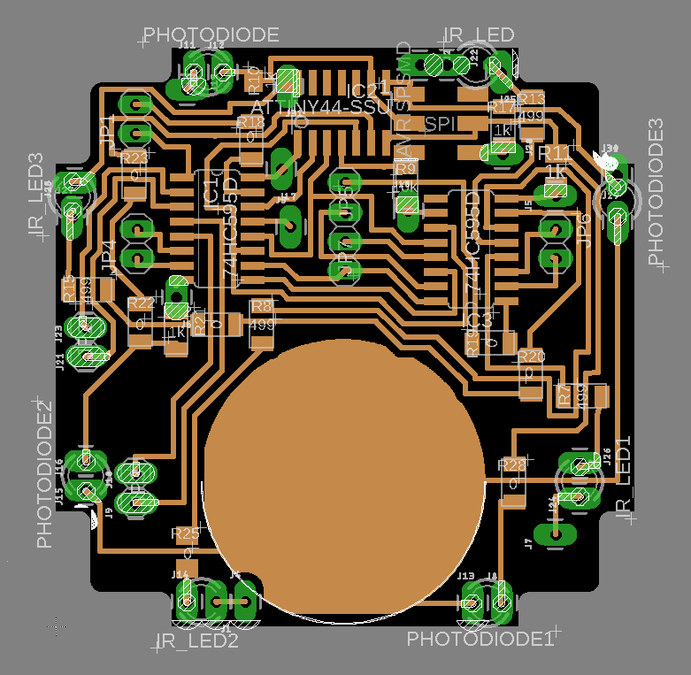
The island on the bottom is reserved for the positive side of the CR2477 coin.The big amount of female pinouts is a result of having a small space and a lot of interconnected parts. By the means of female pinouts the components are routed by having the male pins coming in from the top layer.
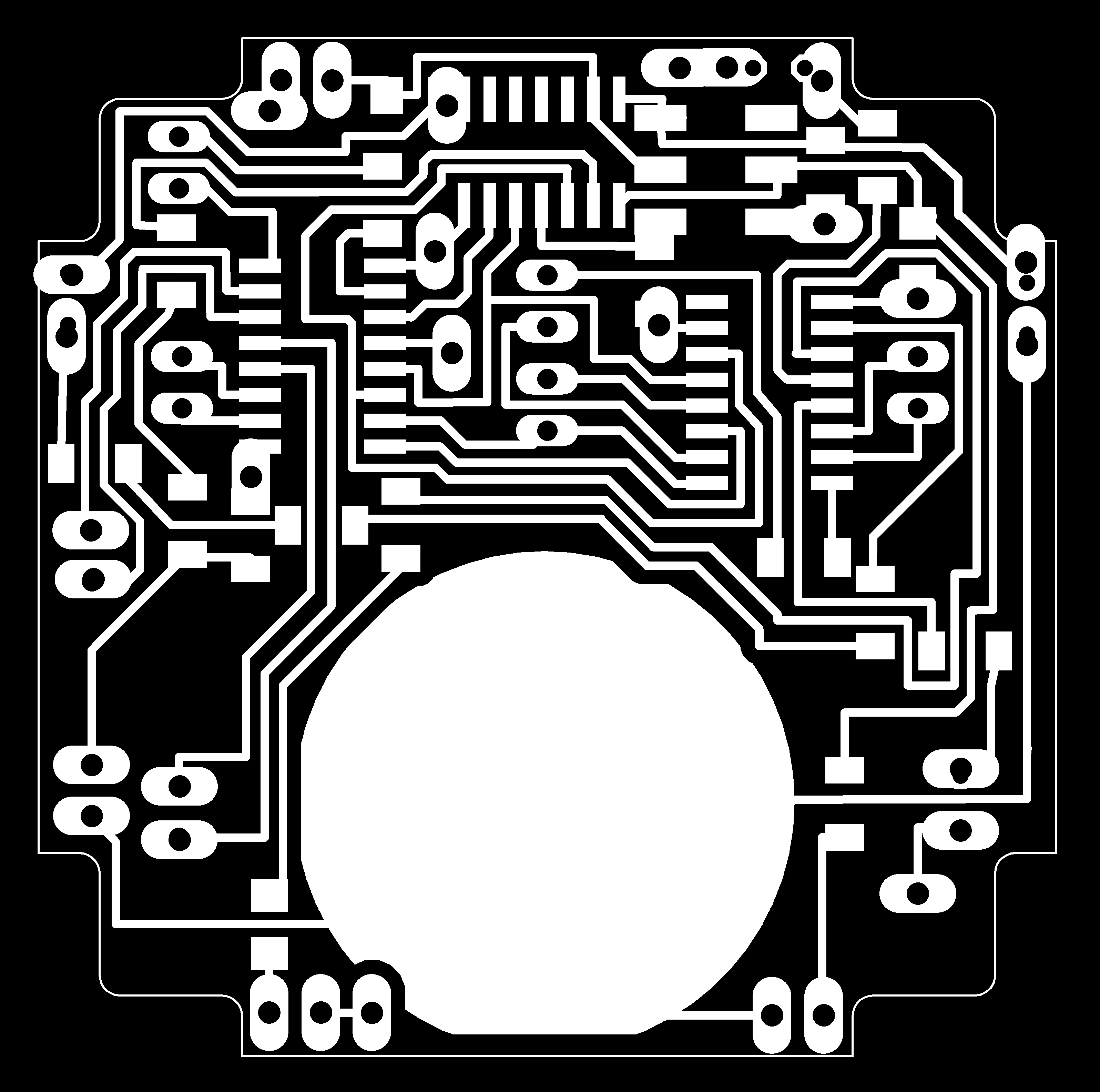
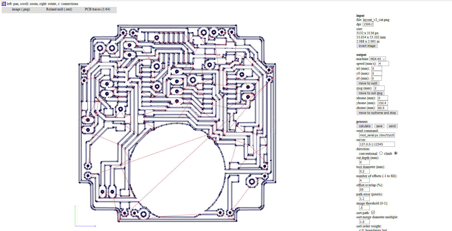
As a result the board is milled with the following setting, details regardin the milling of the board can be found in the electronic production week.
These are the settings used to achieve the milling of the cupper board. To keep in mind that the copper thread has a width of 0.4 mm. This was accomplished using the 0.2-0.5 mm milling tool.
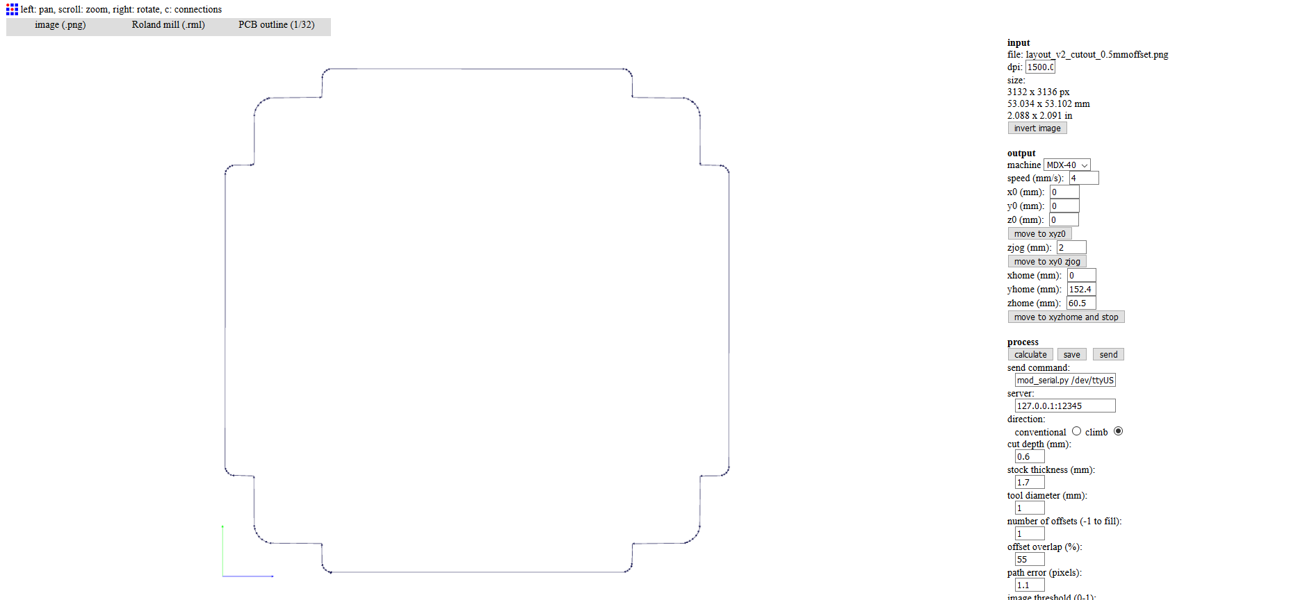
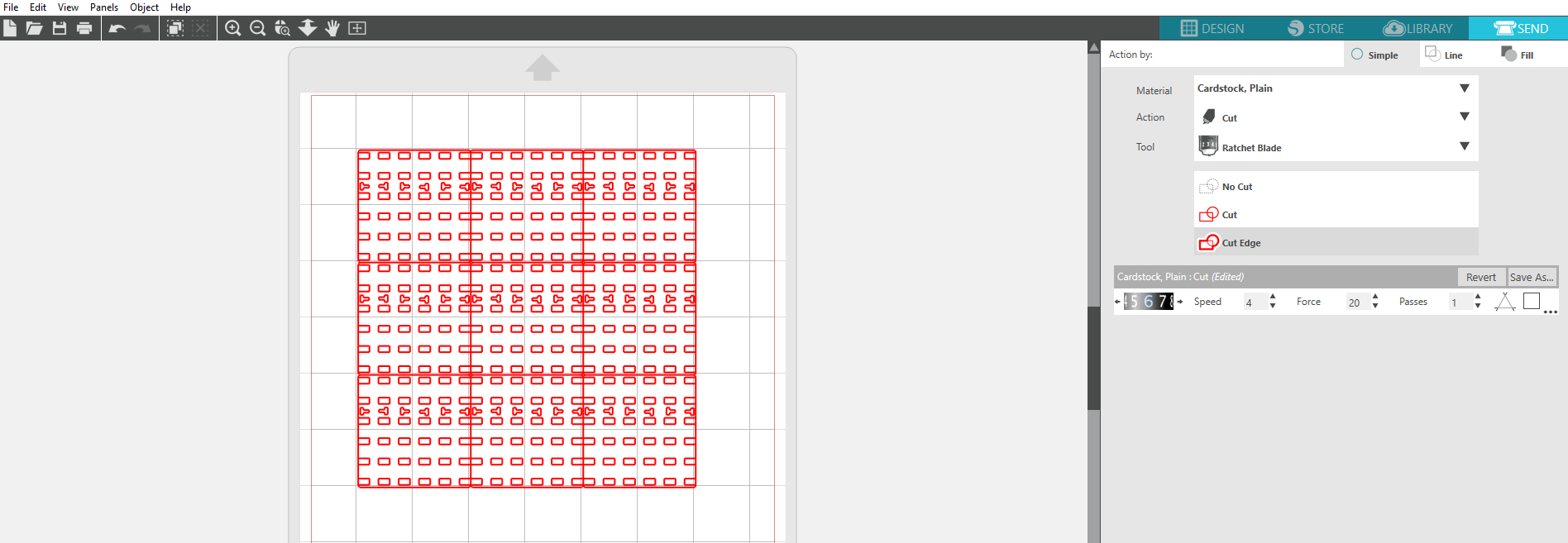
These are the settings used to achieve the cutout of the board.
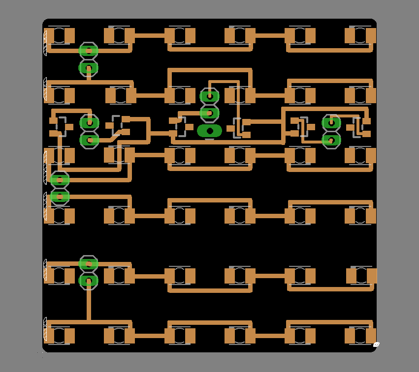
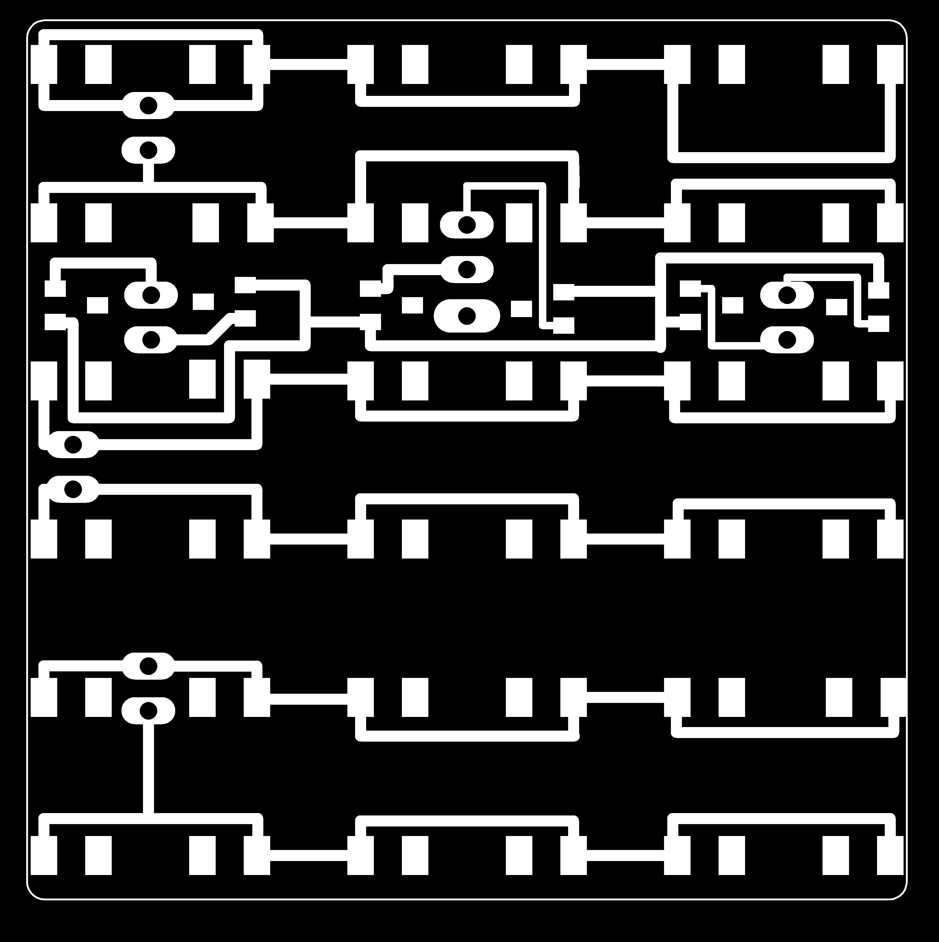
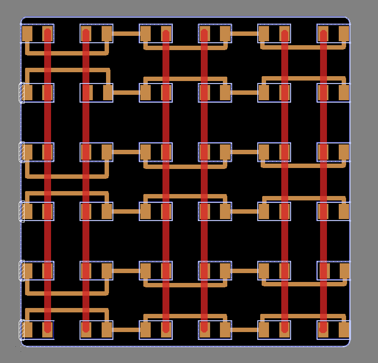
Middle Board.
Because of the an increased amoung of VCC and GND nets, this layer connects all the GND and VCC and brings them down to the bottom board. Also this board passes the controlling pins of the shift registers to the top layer where the LEDs are located.
The resulting negative is flipped vertically in order to then be positioned underneath the top layer.
Same cutting settings are applied to achieve the milling and the cutout.
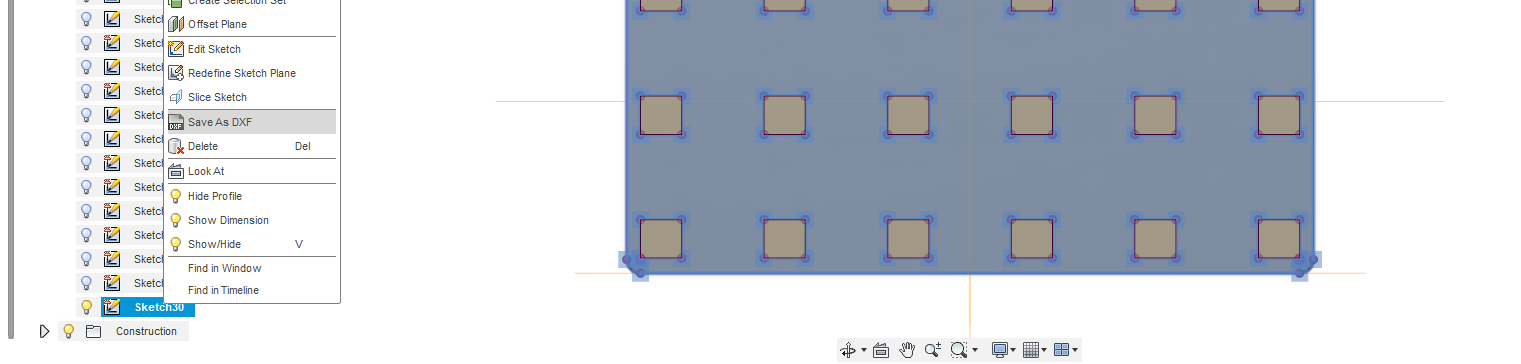
Top Board.
This layer is the top layer of the cube. It hosts:
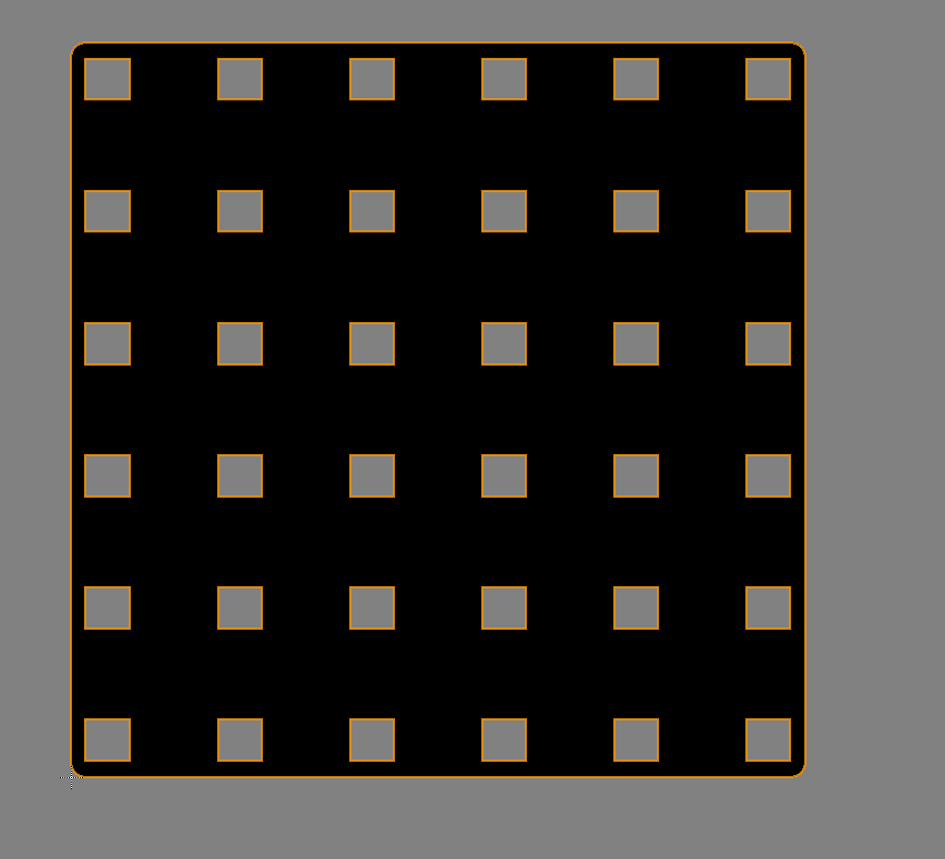
It was created by first exporting the DXF sketch from Fusion 360 model and then importing it into the Eagle board layour.
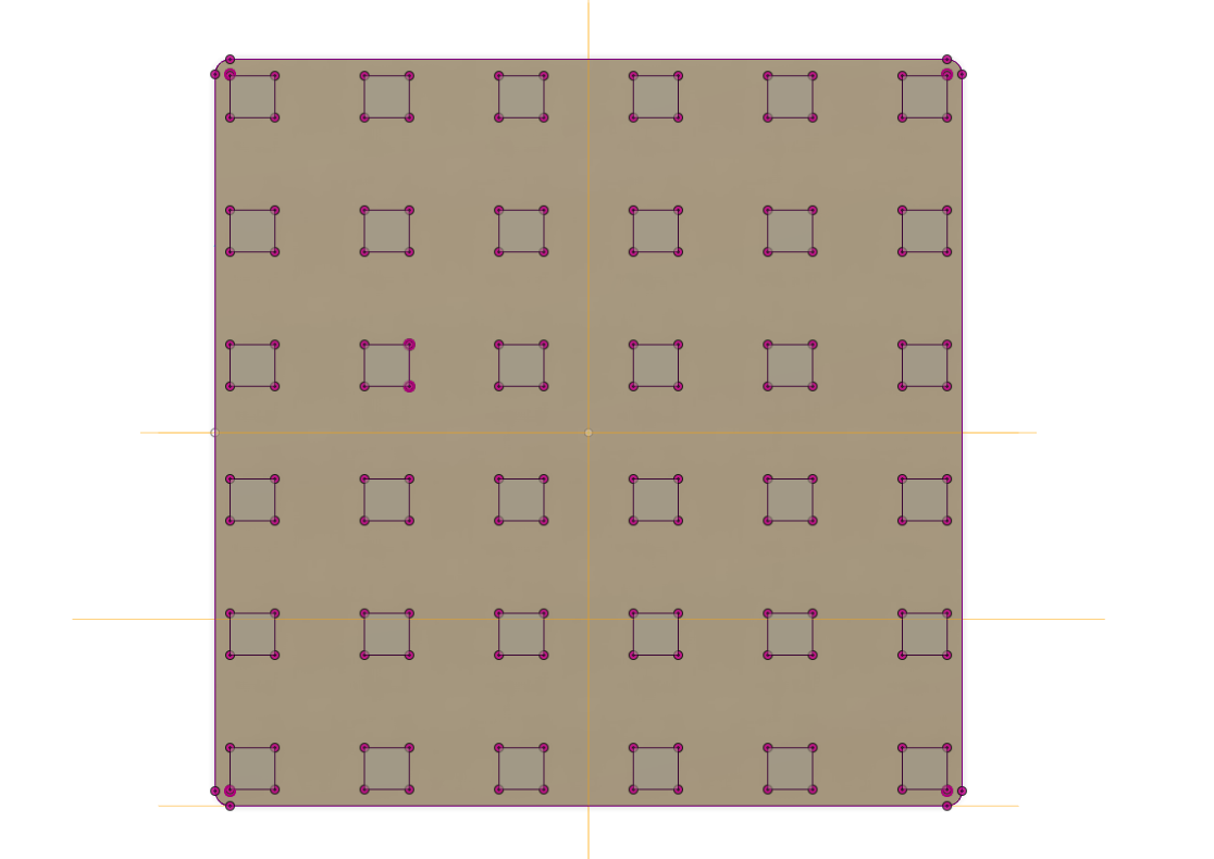
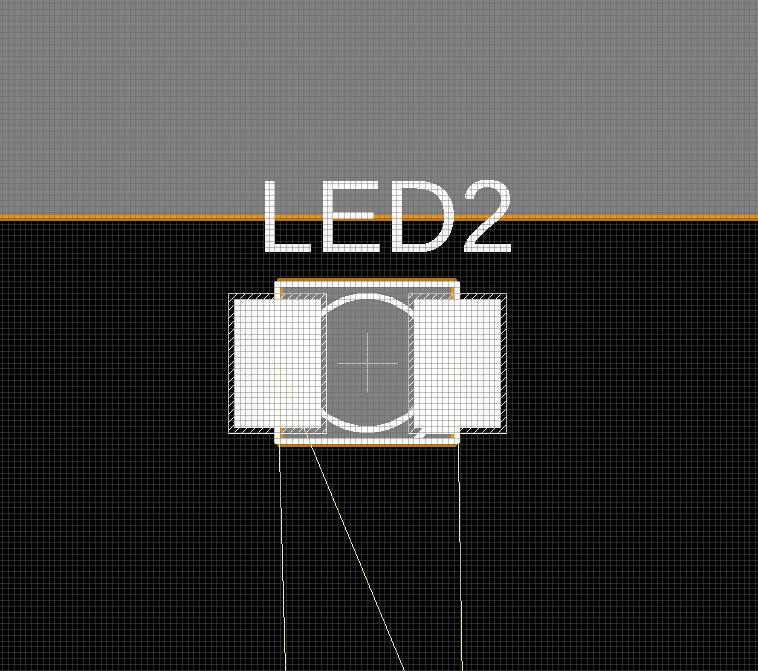
By the means of projecting the faces of the LEDs onto the sketch.
Sketch exported as DXF.
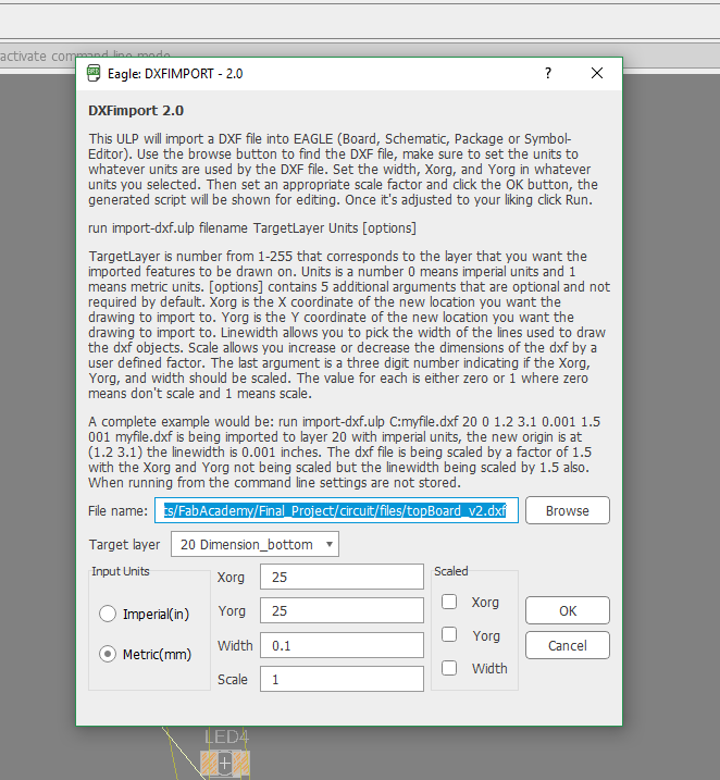
Then imported into Eagle, giving the correct origin point and the board layout and populated. This allows an even spacing of the LEDs.
Same cutting settings are applied to achieve the milling and the cutout.
Vinyl Cut Layer.
A vinyl layer is the last layer from the top that will allow the separation of the LEDs VCC and the GND layers. By importing the DXF file previously generated to create the Top Layer and modifying by enlarging the space for the LEDs and the transistors, we achieve another vinyl layer in blue color.
The red stripes will be made out of copper tape that will be then soldered to the LEDs GND connection.
Using the knowledge from Computer Controlled Cutting week, the vinyl layer is sent to print using the following settings.
Putting Together.
Using the knowledge from the Electronic Production, all the layers are soldered using the components mentioned above.
Resulting boards:
.jpg)
.jpg)
Attiny84 and the shift registers.
.jpg)
Attiny84 and the shift registers.
.jpg)
Female pinouts.
.jpg)
Infrared system.
.jpg)
Battery attached.
.jpg)
Male pinouts for the middle layer. The pins that need to be connected on the top layer are passed through and soldered on the other side, this way the both copper sheets are sticked together.
.jpg)
The leds and transistors are soldered first.
.jpg)
All mounted.
.jpg)
These are the results of the vinyl cutting.
.jpg)
Vinyl cutter is sticked and raws of copper are soldered for the GND.
.jpg)
The system with the LEDs.
.jpg)
Testing the system.