I was late for this weeks work as I had been behind for some of my works. I am however starting to catch up quite well now.
Initially, getting the board up and connected on Eagle took some time because it was completley new territory for me. We had setup a class document as part of our group assignment so I used this as a guidline when I was putting the pieces together.
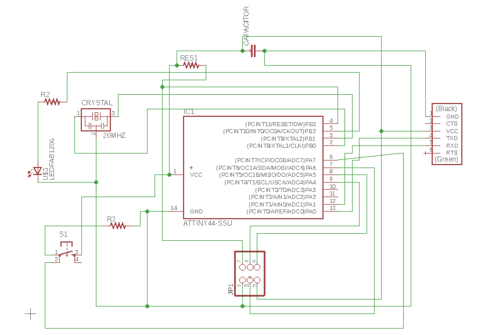
I started by first doing Neil's "Hello World" board design...
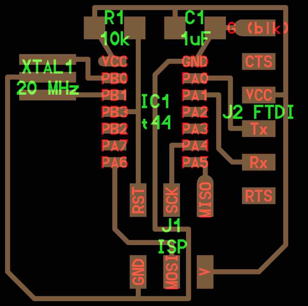
Then I moved onto piecing everything together on both my schematic and then tried adding my extra components (my switch/button, and my LED). Adding the extras was a bit hard at first as I did not quite understand at first how to know where to put what, but Andrew my fab lab college was helpful and showed me his page and explained to me the logic behind it. That for both extra components, they needed to be connected to power, have a resistor attached to regulate the voltage flowing in, and then have the other end of the piece hooked up to the ground.
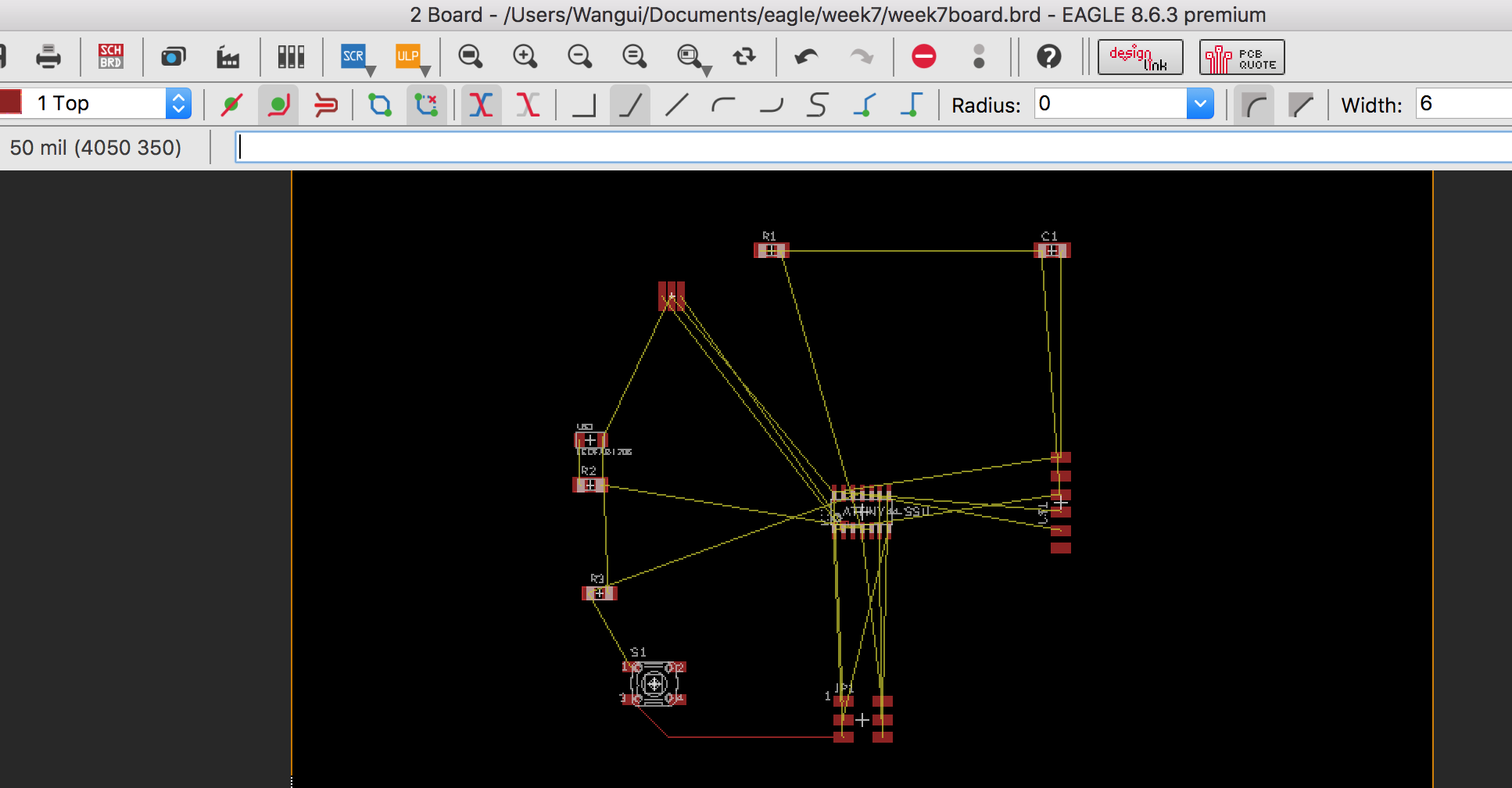
I had attempted to hook everything up on my board, but it got very annoying as I would always end up locked in one place. This means I would have lots of components linked, but then on one I couldn't connect them properly as there was no space left.
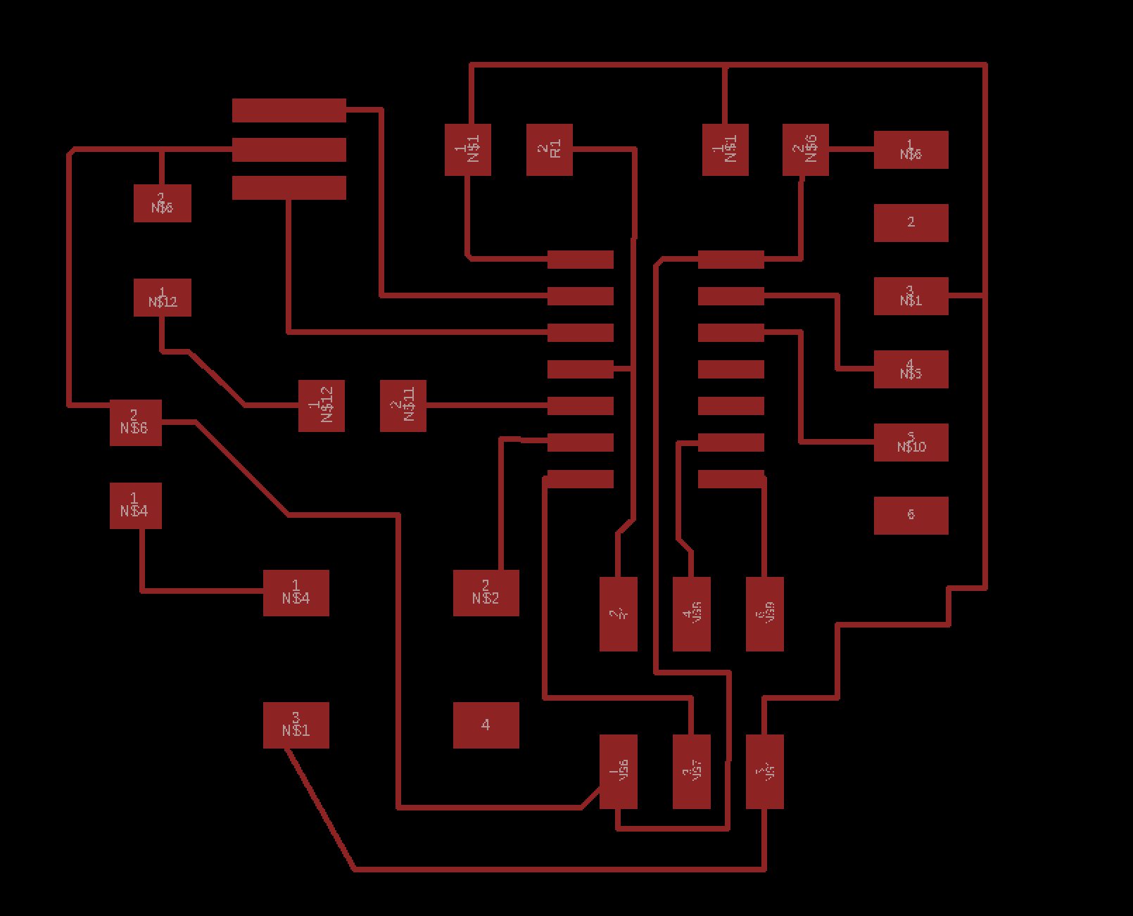
I then decided to delete the connections of the extra components in my schematic and first focus on connecting the inital components - the capacitor, resistor, attiny 44, pin head 2x3, my 20MHz crystal and my 1x6 SMD Male. This made the work flow much easier because there was less to look at. It was after then connecting it that I reconnected my LED and my switch in my schematic, and then added them in where there was appropriate space afterwards. I first had everything spread out so that it was clearer for me to see what was happening. After everything was hooked up properly, I looked into compacting my board so that I would use up as little space as possible in order to "maximize" space and not waste my copper board.
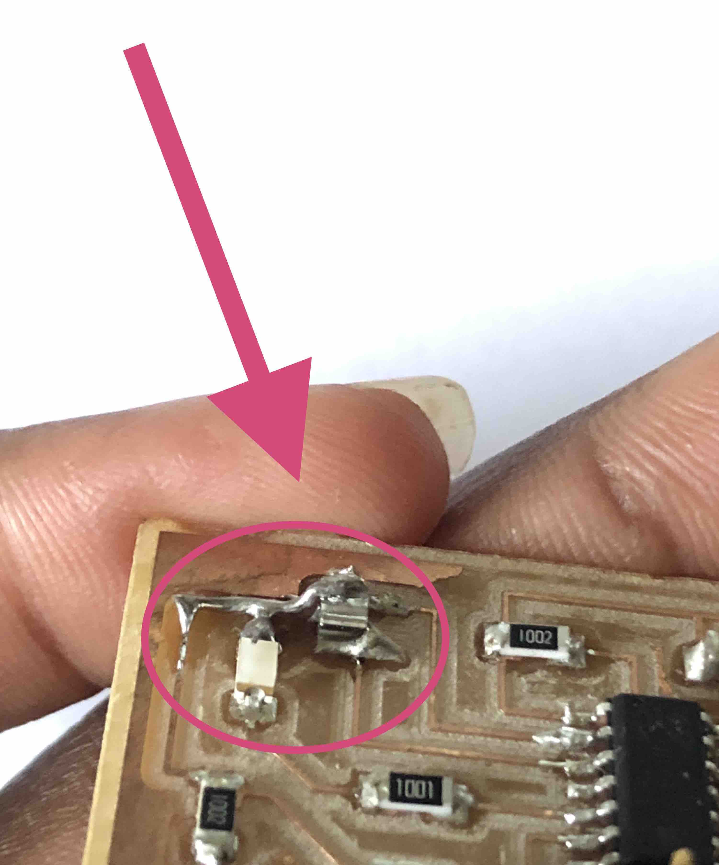
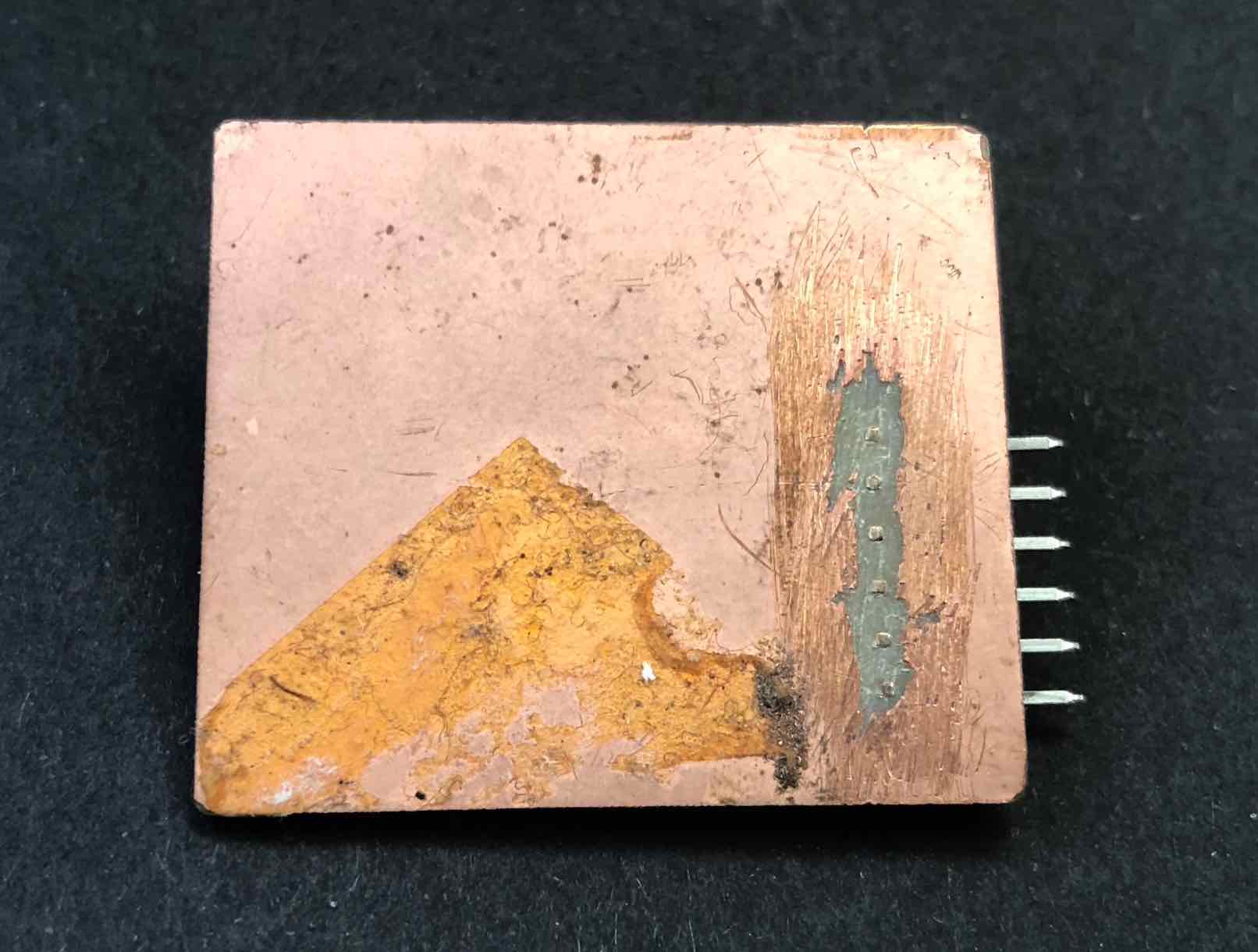
After milling, I luckily enough this time had no issues soldering. Which is great as last time it took 4 times till I got a functioning one. I did run into a minor issue with my crystal again. The problem this time was that I was not able to get the solder to reach the crystal, there was a tiny space left still. This got me to thinking; when I do my board next time and it requires a crystal, I will make the connection between the board and the cystal bigger in the center so that it is easier to solder. Because the line was so thin and getting the middle bit of the crystal is such a delicate job, even after getting help, the connection ended up burning off. Of course the simple and effective solution was to get a wire and solder it onto my board and create that connection. Thankfull it worked, and it doesn't look too terrible.
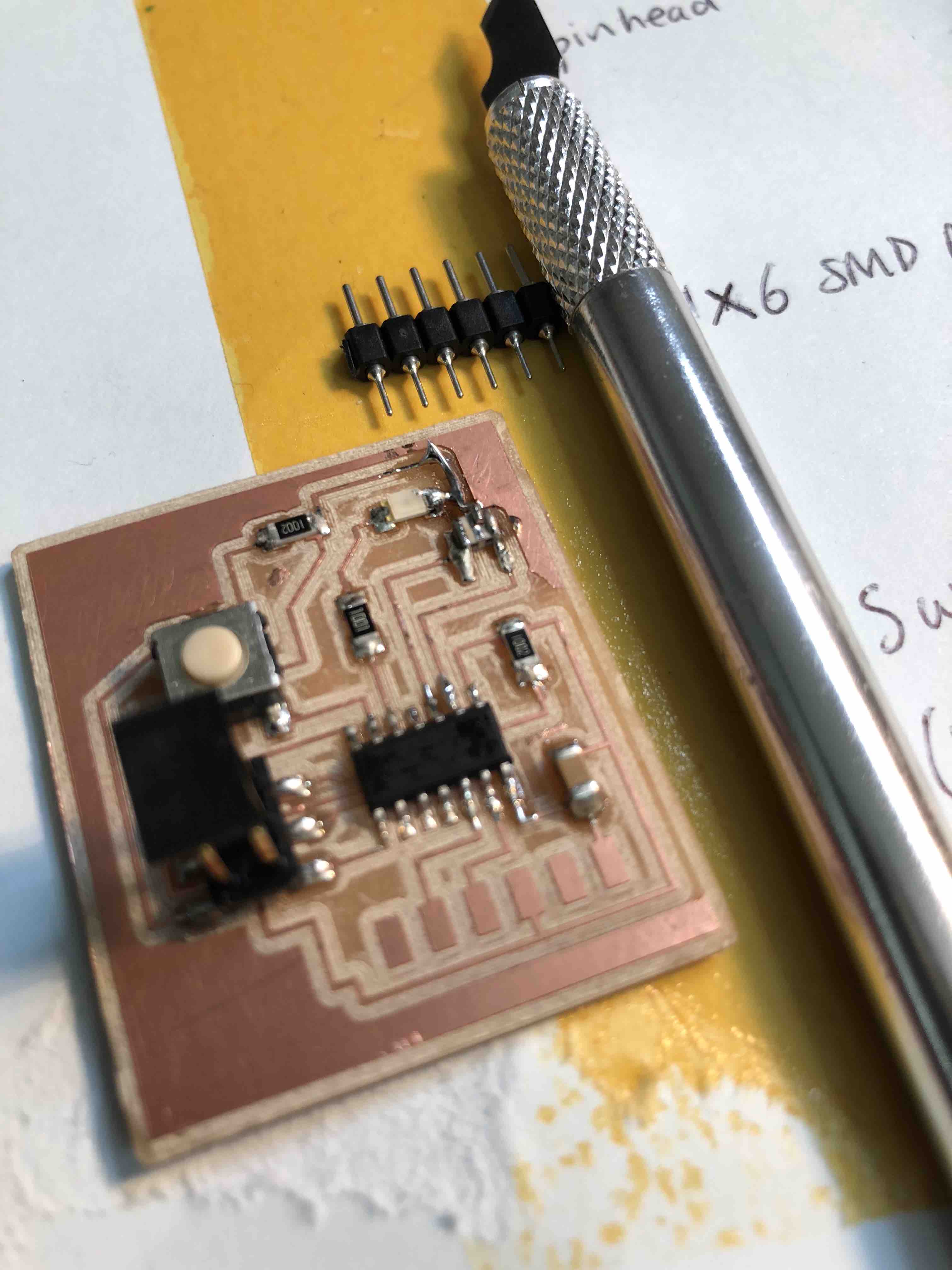
However.., I did run into some small big issues. I say small big because had I not managed to fix it, it would have been big. If you look at the above image, you will see that near the crystal and LED area, it looks ever so slightly wonky. That bit really tested my patience and skills when it comes to soldering (as if I hadn't needed to test it all the other times...). When trying to solder my crystal, the wire pad connecting came off the board. In attempt to save it, the whole wiring came off. Which meant that the connection to the crystal and the LED where thus broken. I had to use wires to then somewhat bridge them together again. It was an intensive job because not only was I "manufacturing" new wire traces I had to make sure that not only was the cystal properly hooked up. To do so I used a sort of "bridge" method. This is because of, well, the lack of trace leading to the crystal now, and the fact that the solder needed to join the middle part of the crystal, and again, with lack of trace there, the only solution was to carefully solder the wire to the middle trace without and of the wire or solder touching the sides of the crystal.
It wasn't my best work I do have to admit, but it got the job done.
Having done so many boards up to this point, I feel confident enough to say that I believe my soldering skills have become much better as the baord looks quite neat and I'm not having to use as much solder in order to effectively solder my components onto my board.
As things were running so smoothly, I decided to take a risk and instead of using my 1x6 SMD and decided to substitute it for the more "longer life" right angle through 1x36 Header Male (which I cut to have 6 pins). It meant having to drill holes into my board which was scary because it could have easily gone wrong if I used the wrong drill or the holes didn't match up properly. What was done was drilling one hole in to test if it fits fine, then using that drilled hole, placing the bit over that hole and placing the other feet of the header pins on the other pads, taking a pointed knife, and making a small hole where they touched. This would, and did, ensure that when the other holes were drilled, that they would go into the right holes and the 6 feet would all fit in fine. It was then just a simple matter of soldering them into place. Thankfully it went well and looks fine now.
After doing this though, it occured to me that the back of my board had copper all over it. Not very helpful!
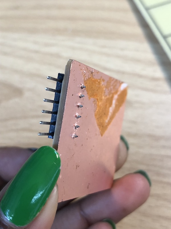
So I took a knife and bascailly scratched the copper area around the pins so that the current flow doesn't leave.
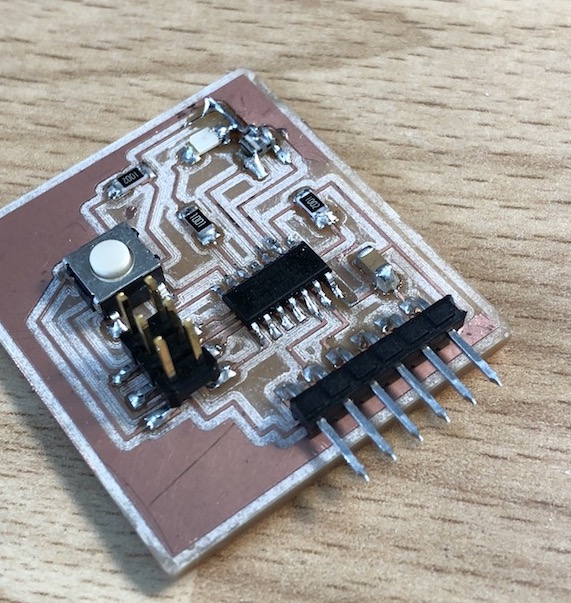
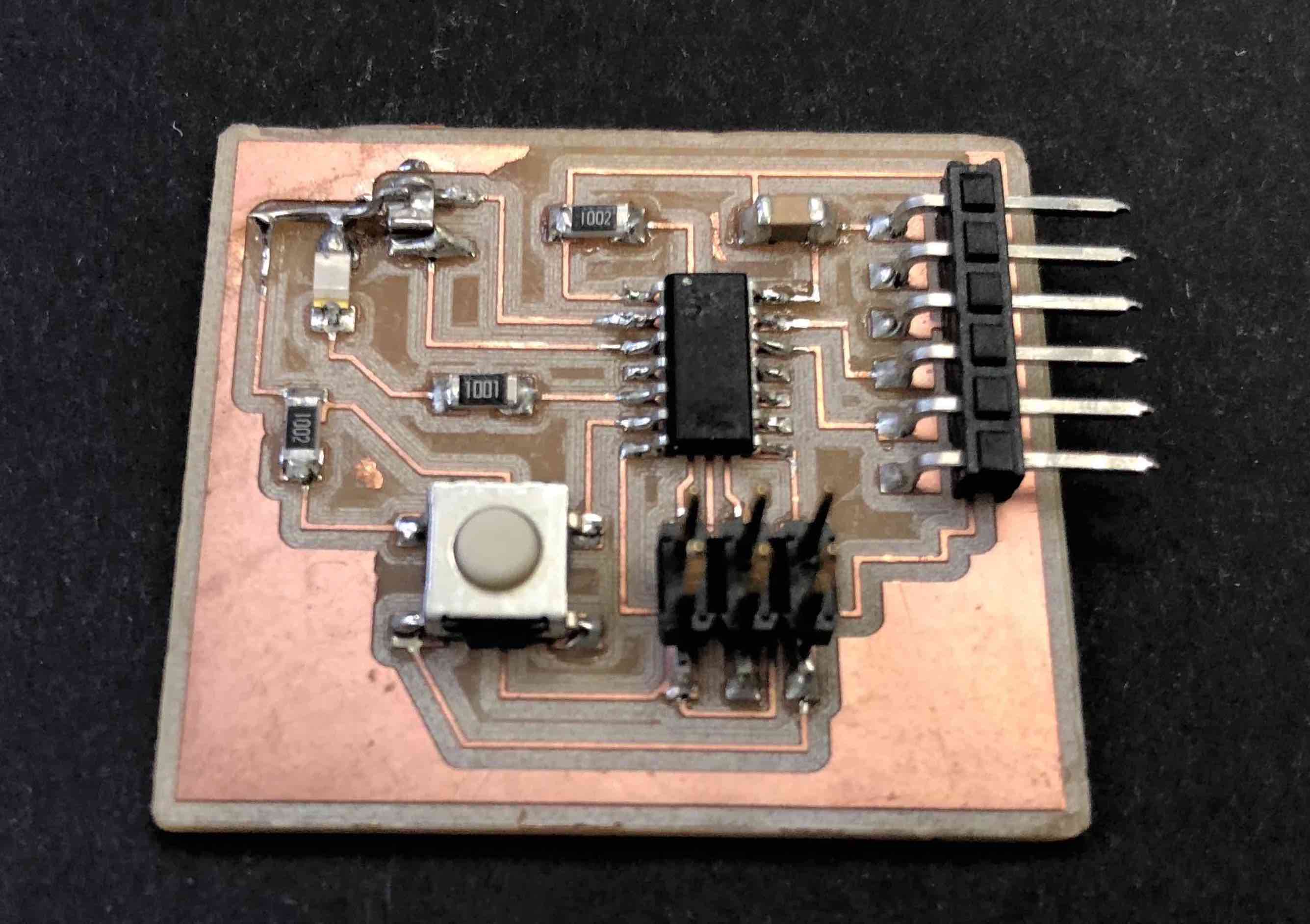
This is is how my board looks now...
Andrew Sleigh's page for this week helped me quite a bit when it came to the LED section because I was constatly confusing myself
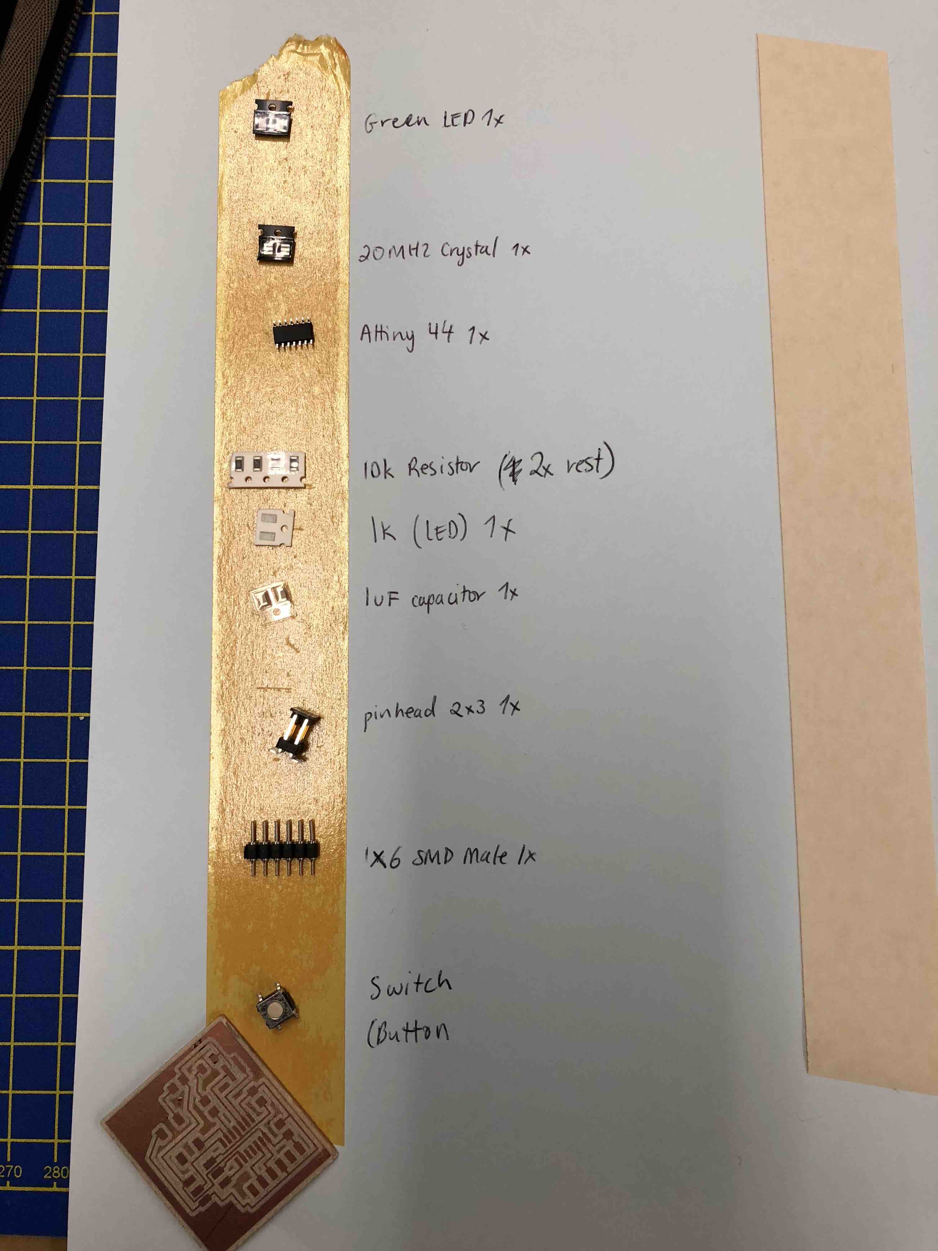
Components used:
Eagle was scary. Not even going to lie. Scariest program I've used yet. It's so blank and empty and so many buttons and options...initially I was a bit concerened that we were to somehow learn to use it within a week not to mention the time that would be required for soldering and testing! Luckily in the end it wasn't so bad and I'm better at it. But I can say for sure that being able to use it with ease will require time and investment...in other words lots of bonding time.
I found this very helpful link by Fab Academy: Introduction to Eagle, where they outline a step-by-steo guide on getting started in Eagle.
As a group we also created a google doc documenting how to create our first board in Eagle (click here)
Adding the fab folder of components
First things first, in order to start adding components to create my board on Eagle, I needed the correct components. This is an essential step beacause if I use incorrect components, when I go to export the .png of the board and then later cut it, it will not match up to the components I intend to use.
Use this link to download the fab library required.
Adding and connecting components
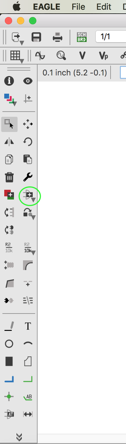
To add components you can either use the button shown below to add in components from folders, or go into the top search bar and simply type "Add". This is what I did for the most part.
Adding from toolbar
Adding from seach bar
// //
//
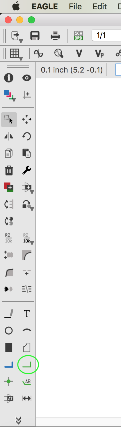
To connect them you simply use the green line button on the side coloum of tools.
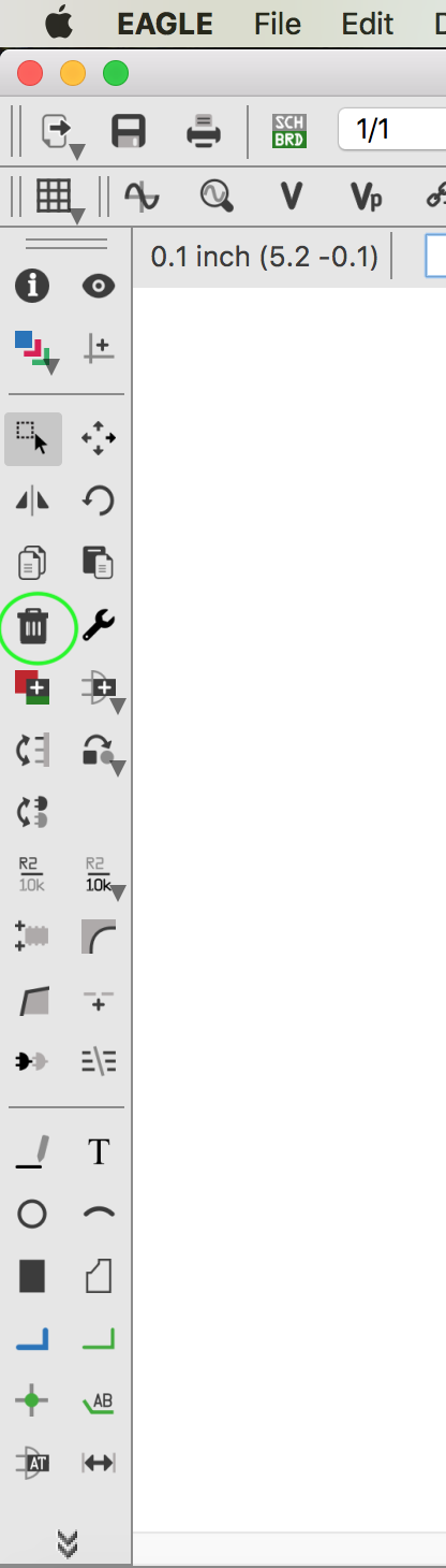
To then delete them, say you accidentally connected two traces together that should be together, or you want to put it elsewhere, you click the trash can button on in the tool bar on the left side.
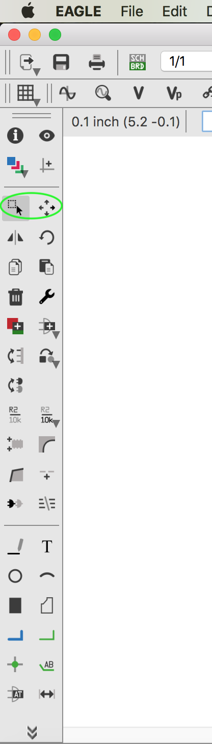
You can use the top most buttons to select and move around your traces. You can select a single trace to move a whole "right angle"/two lines connected. However, only the first one allows you to select a whole area.
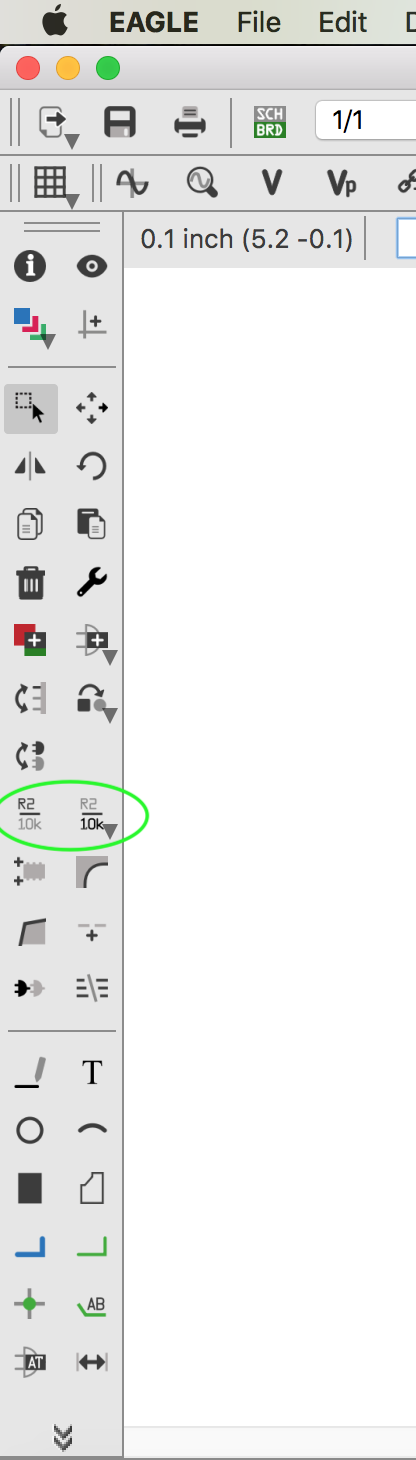
you can use these two to label traces. This the right one labels the name of the trace, the left one the type of component, eg. if the component is a 100 Ohm resistor. This is especially helpful when later on in your board creation stage, you are trying to organise things as you can see what is what, and if you zoom into your trace, you can easily figure out what role each trace has. For example is one trace is all VCC or GND (ground).
Creating Board
As previously mentiined, I started by first doing Neil's "Hello World" board design, and piecing everything together on both my schematic and then added my extra components (my switch/button, and my LED). This made it easier to understand where to begin and the flow, especailly being new to Eagle. As my intial attempt at Eagle when creating my board did not go smoothly. I ended up having a very hard time figuring out how to connect my components, almost always ending up in a "land-locked" position I couldn't get out of. Granted I could have used zero ohm resistors as jump resistions, but at the time, I was still comprehending what was was, and didn't even know or understand zero ohm resisitors. Which is funny because I have done physics so I know. But I think it was one of those cases where you know something, but just know it because you know it, not because you are actually in a situation using it. If that makes any sense to you.
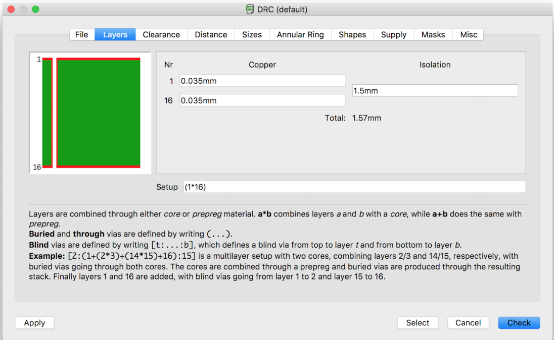
Design Rules: Making sure traces are thick/thin enough
On the Board view in Eagle, open the Design rules window (Tools menu > DRC...) and set them to the following
Benefits of a Microcontroller Datasheet
Ok. So I admit. It's good stuff. I love to read, but as soon as someone says I have to read something, it instantly puts me off and it seems like such a darn chore. Same in school. Once in a while it seems good and I'll do it anyways, but the other times?....Well...Nah. BUT THIS! This was worth it. It really did and continued to help me with the rest of my projects. It's helpful because it's almost like...a dicitonary I guess. Except this time you don't actually know the word you're looking for...so a reverse one? Although if you know what you're looking for even better. If I was unsure about how much memory my microcontroller had, it could tell me. PIN CONFIFURATION! Now that is always helpful because I can't always remember where what pin in connected to. So instead of having to pull up eagle which on my laptop can sometimes run a bit slow, I can pull out the data sheet and it'll tell me where's what and I can just simply follow my traces and compare. Easy. Peasy....just wish it was a bit colorful. XD Can't have it all!s
Tips and tricks corner
My personal tip is to start of making sure you decide on a trace size, and then if need be, edit it later. This is because then you'll spend less time trying to move around your components, and will have more space and will therefore require less jumper resistors.
Another helpful tip is ORGANIZATION!!!...I cannot stress that enough. This applies to both your schematic and the board. It is helpful for the schematic because when you decide to go back and edit it, say perhaps you've realized you can use or need to use a lower or higher resistor after you've compelted some testing, or you want to modify a board for another purpose, having the schematic neat helps save a lot of time. This is something I've found. Initially I did not pay much attention to how organized it was, but then it made going back to it very tedious. As for the board, organization is key because of space. There is no need to create a big board and waste lots of copper. Not only that, but remaining organized can help when you are attatching things to your board later and it can save on milling time. It also will result in neededing to use less jumper 0 ohm resitors. And lastly, both cases - it makes it easier for others to comprehend what you were doing, or even yourself later on when you decide to go back to an old board. :)
My global evaluator Bas kindly pointed out an improvement I could make which is to use the pull-up resistor internally found in the Atting44 chip instead of using its own resistor.
I found this page to be quite helpful to alleviate some of the initial frustration Eagle "blessed" me with Creating Components in Eagle (Almost) Frustration-Free .
This is a list of commands to use in Eagle.
To be very honest, I only ever used the "add" in Eagle. But the above two links proved helpful when I needed that extra helper.
This weeks homework:
And for those extra brownie points...